Method of fabricating dual-band type-II superlattice detectors based on p-B-p design

a detector and superlattice technology, applied in the direction of sustainable manufacturing/processing, semiconductor devices, climate sustainability, etc., can solve the problems of inassb bulk materials that cannot be used in high-performance long-wave infra-red photodetectors, t2sls doped n-type will inevitably have limited quantum efficiency,

Active Publication Date: 2015-06-23
HRL LAB
View PDF3 Cites 10 Cited by
  • Summary
  • Abstract
  • Description
  • Claims
  • Application Information

AI Technical Summary

Benefits of technology

[0011]In another embodiment of the principles of the present invention comprises a Type II Superlattice Dual Band Photodetector comprising: a first absorber layer adapted to absorb light with a wavelength between 3 microns and 14 microns; a second absorber layer adapted to absorb light with a wavelength between 3 microns and 14 microns; and a barrier layer means disposed between the first absorber layer and the second absorber layer for eliminating a depletion region between the first absorber layer and the second absorber layer for the dual band Photodetector.

Problems solved by technology

InAsSb bulk materials do not translate well to high performance Long Wave Infra Red photodetectors due to the lattice mismatch.
However, due to the poor diffusion of holes in T2SLs, absorber layers need to be doped p-type so that the higher mobility electrons are the minority carriers.
T2SLs doped n-type will inevitably have limited quantum efficiency.

Method used


Image

  • Method of fabricating dual-band type-II superlattice detectors based on p-B-p design
  • Method of fabricating dual-band type-II superlattice detectors based on p-B-p design
  • Method of fabricating dual-band type-II superlattice detectors based on p-B-p design

Examples


Embodiment Construction

[0021]In the following detailed description, only certain exemplary embodiments of the present invention are shown and described, by way of illustration. As those skilled in the art would recognize, the described exemplary embodiments may be modified in various ways, all without departing from the spirit or scope of the principles of the present invention. Accordingly, the drawings and description are to be regarded as illustrative in nature, and not restrictive.

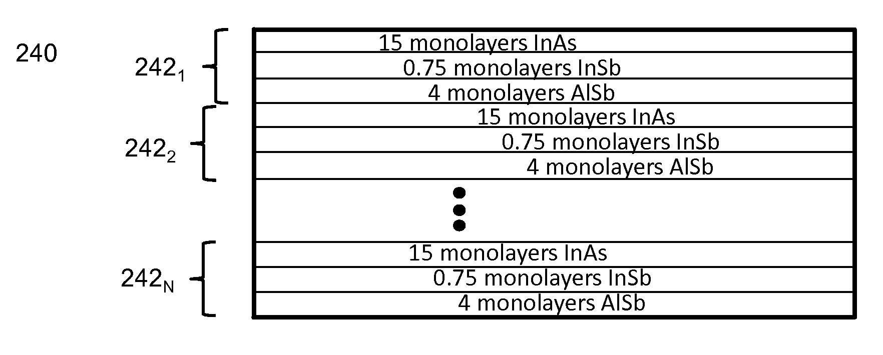
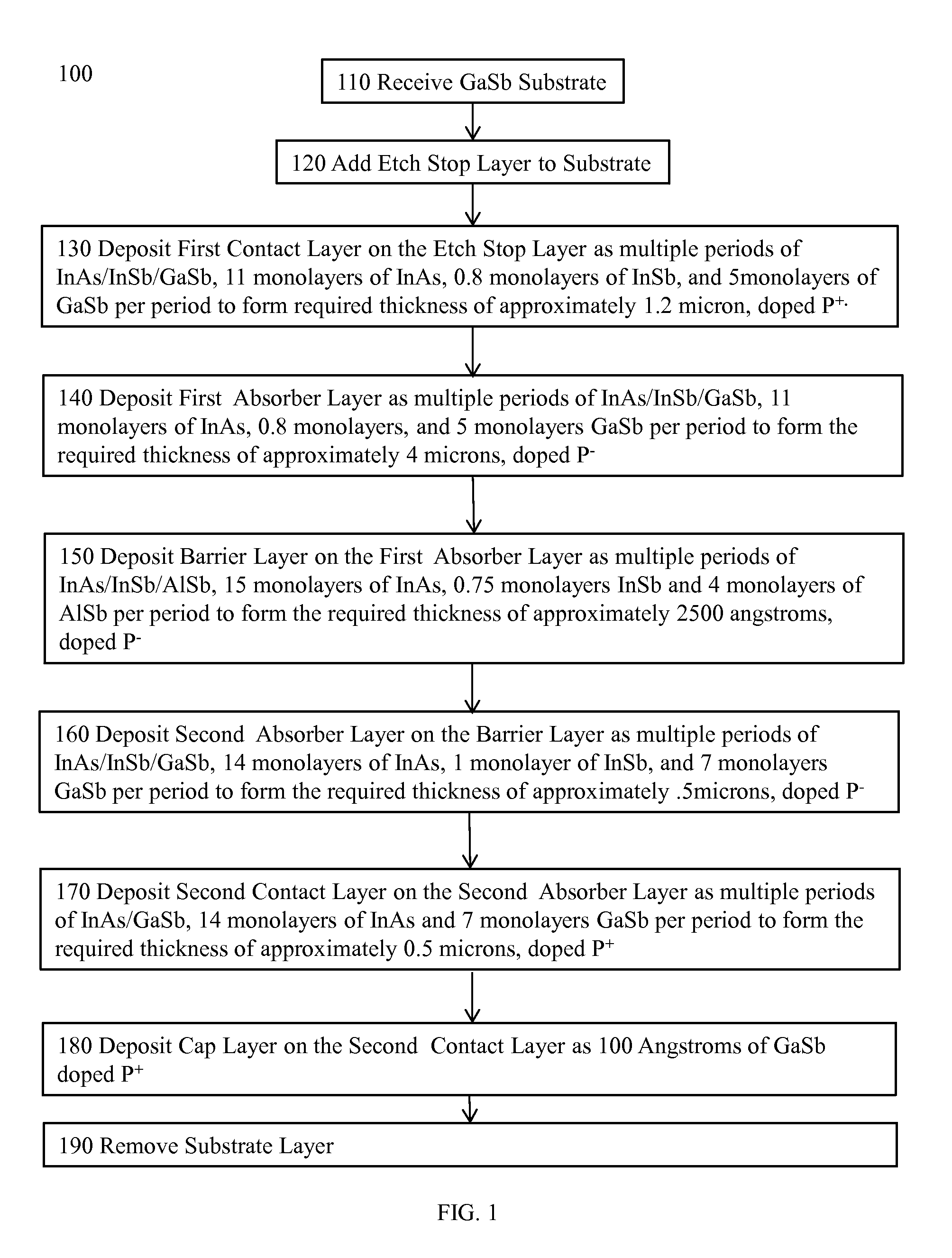
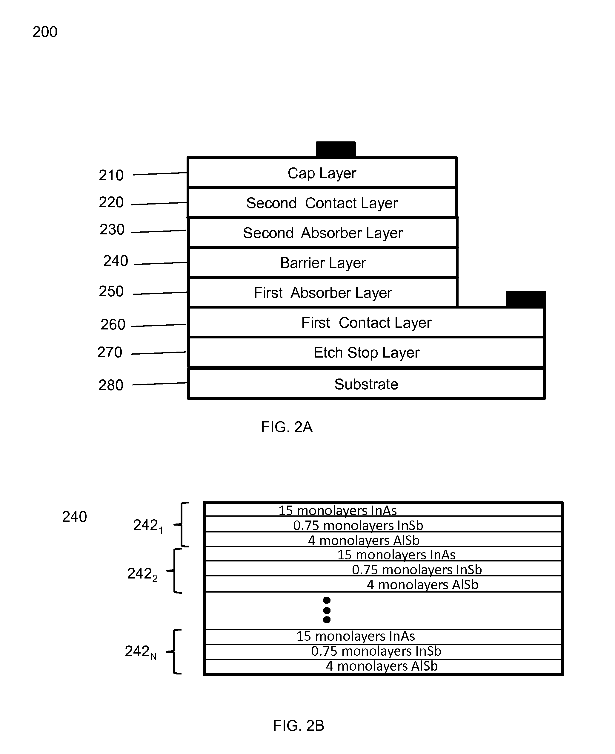
[0022]The problems described in the background section are at least partially solved by the principles of the present invention, including, by P type doping of a multiple layer barrier structure. The structure of an embodiment of the principles of the present invention uses a barrier structure comprising multiple layers, chosen to lattice match to the absorber layer above and below, and to present a transition in the conduction band from a first absorber layer to a second absorber layer across the barrier layer such that the...


PUM


Abstract

A dual-band infrared detector structure based on Type-II superlattices (T2SL) has been developed and experimentally validated. The structure according to the principles of the present invention is designed for a single Indium bump architecture and utilizes a T2SL barrier design that omits the traditional p-n junction region. The barrier design comprises multiple periods where each period comprises multiple monolayers doped P type. By selecting the composition, number of monolayers per period and number of periods, a transition region is created in the conduction band between a first absorber layer and a second absorber layer that allows operation at low biases (<100 mV for both bands) and exhibits a dark current density in the longer wavelength band comparable to that obtained with single-color detectors.

Description

[0001]This application is a divisional application of Ser. No. 13 / 351,997 filed Jan. 17, 2012. This application claims priority to provisional application 61 / 433,600 filed Jan. 18, 2011 titled Dual-Band Type-II Superlattice Detectors Based on p-B-p Design. Provisional application 61 / 433,600 is incorporated by reference herein.STATEMENT REGARDING FEDERALLY SPONSORED RESEARCH OR DEVELOPMENT[0002]This invention was made with Government support under Contract No. FastFPA S09-102166 awarded by the US Government. The Government has certain rights in the invention.FIELD OF THE INVENTION[0003]The present technology relates to an apparatus and method for improving the sensitivity of a dual band photodetector while also reducing the dark current.BACKGROUND OF THE INVENTION[0004]InAsSb bulk materials do not translate well to high performance Long Wave Infra Red photodetectors due to the lattice mismatch. Some work has been done on using nBn designs with Type II Superlattice (T2SL) absorber lay...

Claims


Application Information

Patent Timeline
Patent Type & Authority Patents(United States)
IPC IPC(8): H01L31/00H01L31/18H01L31/0352
CPCH01L31/035236H01L31/18H01L31/09H01L31/1013H01L31/184Y02P70/50H01L31/02016H01L31/065H01L31/109H01L31/11Y02E10/544
Inventor NOSHO, BRETT ZRAJAVEL, RAJESH DSHARIFI, HASANTERTERIAN, SEVAG
Owner HRL LAB
Why Eureka
Try Eureka