Low-noise low-distortion signal acquisition circuit and method with reduced area utilization

a signal acquisition and low-noise technology, applied in the field of sample and hold circuits and sampling systems, can solve the problems of signal recovery methods adding their own non-idealities and design burden on the whole data acquisition (daq) chain, and the quality cannot be recovered afterwards, and the prior art suffers from a different potential problem

Active Publication Date: 2015-07-07
CAES COLORADO SPRINGS LLC
View PDF11 Cites 9 Cited by
  • Summary
  • Abstract
  • Description
  • Claims
  • Application Information

AI Technical Summary

Benefits of technology

[0007]According to another embodiment of the present invention a sample and hold amplifier includes an operational amplifier having a negative input, a positive input coupled to ground, and an output, a non-linear capacitor having a first terminal, and a second terminal coupled to the negative input of the operational amplifier, a linear capacitor having a first terminal, and a second terminal coupled to the negative input of the operational amplifier, a first switch coupled between the first terminal of the non-linear capacitor and the output of the operational amplifier, a second switch coupled between the first terminal of the non-linear capacitor and ground, a third switch coupled between an input node and the negative input of the operational amplifier, a fourth switch coupled between a first terminal of the linear capacitor and ground, and a fifth switch coupled between a first terminal of the linear capacitor and the output of the operational amplifier. The first, third, and fourth switches are configured to switch according to a first phase signal. The second and fifth switches are configured to switch according to a second phase signal. The input node constitutes a virtual ground useful for the biasing of, and receives an input current signal provided by, a photodiode. The sample and hold amplifier further includes a reset switch coupled between the negative input of the operational amplifier and the output of the operational amplifier, wherein the reset switch is configured for receiving a reset signal. The sample and hold amplifier may further include a linear load capacitor coupled to the output of the operational amplifier through a switch configured to switch according to the second phase signal.
[0008]The foregoing and other features, utilities and advantages of the invention will be apparent from the following more particular description of an embodiment of the invention as illustrated in the accompanying drawings.

Problems solved by technology

In fact, once the signal under observation in the external world has been corrupted by either adding noise onto it or generating spurious harmonics, its quality cannot be recovered afterwards, unless other parametric information about the input were already known; and the signal recovery method will add its own non-idealities and design burden on the whole data acquisition (DAQ) chain.
However, this simple design choice often conflicts with the speed and especially with the area requirements of an integrated solution, in particular when the sampling circuit is employed at the front-end of a multi-channel system such as the ones found in imaging and / or bio-medical machines, which can range from 2 to 256 or more channels, activated simultaneously or in a time-staggered fashion.
Besides the issue of area, the aforementioned prior art suffers from a different potential problem: the capacitance non-linearity vs. voltage, often quantified by voltage coefficients VC1 [ppm / V] and VC2 [ppm / V2], respectively for linear and quadratic dependence of the capacitance Cs on the input signal (charge q(t)).

Method used


Image

  • Low-noise low-distortion signal acquisition circuit and method with reduced area utilization
  • Low-noise low-distortion signal acquisition circuit and method with reduced area utilization
  • Low-noise low-distortion signal acquisition circuit and method with reduced area utilization

Examples


Embodiment Construction

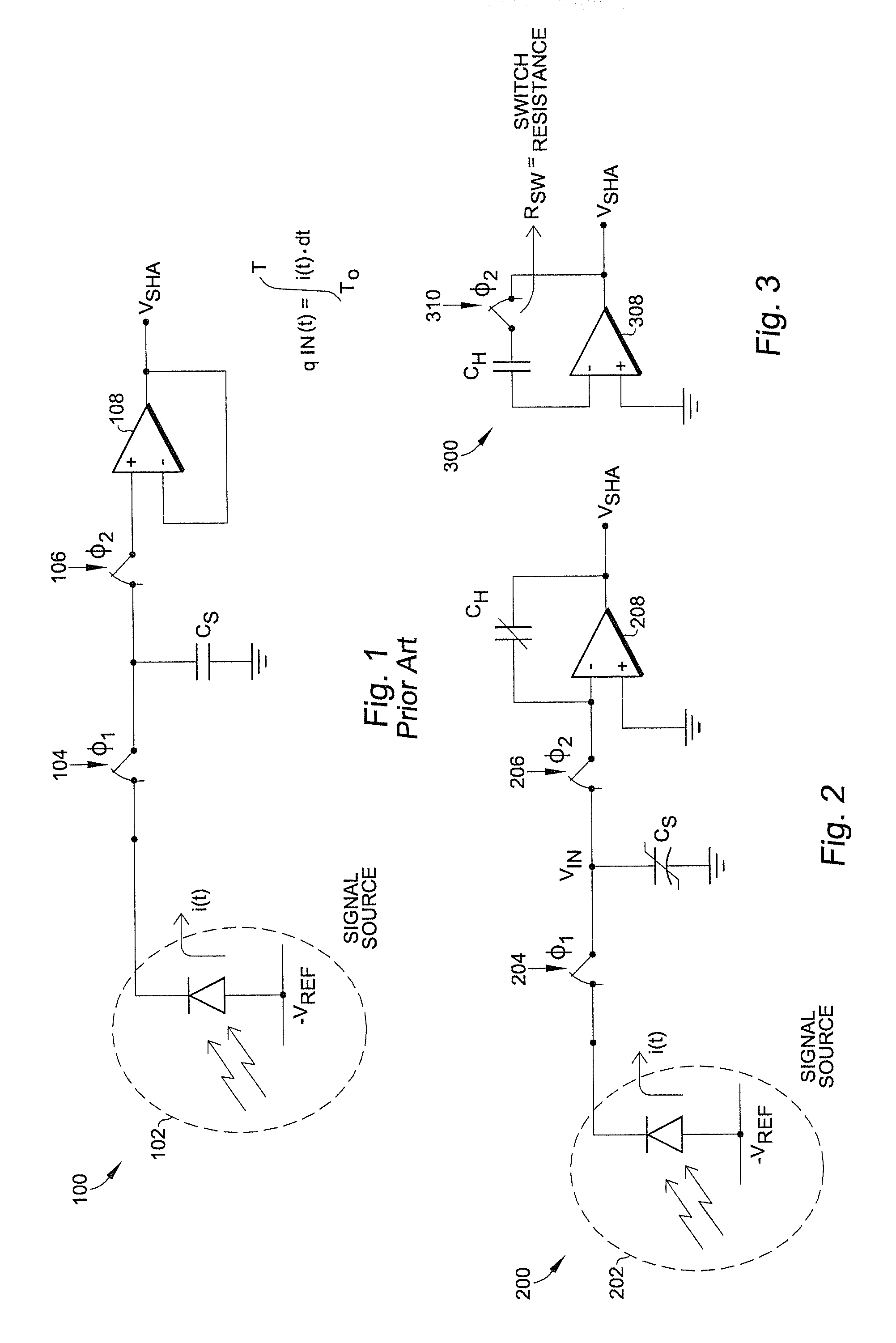
[0017]Referring now to FIG. 2, a sample and hold amplifier 200 according to the present invention includes a sampling capacitor circuit including a non-linear capacitor Cs, a first switch 204 and a second switch 206. The first switch is switched with a first phase signal, and the second switch is switched with a second phase signal. The sampling capacitor circuit is coupled to the negative input of an operational amplifier 208. The positive input of operational amplifier 208 is coupled to ground. The output of operational amplifier 208 provides the voltage output signal VSHA. The input current is provided by a photodiode 202, although the input current can also obviously be provided by other sources if desired.

[0018]As in the prior art, the signal current i(t) is integrated on a capacitor CS which can be made large to minimize silicon area and kT / CS noise. In a practical implementation as an I.C. (integrated circuit), CS will necessarily be non-linear (as indicated in figure by its ...


PUM


Abstract

A sample and hold amplifier includes an input node for receiving an input current signal, a non-linear sampling capacitor circuit having an input coupled to the input node, an operational amplifier having a negative input coupled to an output of the non-linear sampling capacitor circuit, a positive input coupled to ground, and an output for providing a sample and hold voltage signal, and a linear capacitor coupled between the negative input and the output of the operational amplifier. The non-linear sampling capacitor includes a non-linear capacitor coupled between an intermediate node and ground, a first switch coupled between the input and the intermediate node configured to switch according to a first phase signal, and a second switch coupled between the output and the intermediate node configured to switch according to a second phase signal.

Description

CROSS REFERENCE TO RELATED APPLICATION[0001]The present application relates to and claims priority of U.S. provisional patent application (“Provisional Application”), Ser. No. 61 / 929,867, filed on Jan. 21, 2014. The disclosure of the Copending Provisional Application is hereby incorporated by reference in its entirety.FIELD OF THE INVENTION[0002]The present invention is related to sample and hold circuits and sampling systems including a plurality of sampling channels, each channel including a sample and hold circuit.BACKGROUND OF THE INVENTION[0003]Virtually all digitization systems interacting with the analog world are faced with the challenge of acquiring an external input signal with a circuit that minimizes noise and distortion. In fact, once the signal under observation in the external world has been corrupted by either adding noise onto it or generating spurious harmonics, its quality cannot be recovered afterwards, unless other parametric information about the input were alr...

Claims


Application Information

Patent Timeline
Patent Type & Authority Patents(United States)
IPC IPC(8): G11C27/02H03F3/45H03M1/36
CPCG11C27/026H03F3/45H03M1/36H01L31/02002H03F1/08H03F1/083H03F3/08H03F3/087H03F3/45076H03F3/45475H03F2200/129H03F2200/156H03F2200/45H03F2203/45444H03F2203/45514H03M1/1215
Inventor ZANCHI, ALFIOHISANO, SHINICHI
Owner CAES COLORADO SPRINGS LLC
Why Eureka
Try Eureka