3C-SiC transistor

a technology of 3c-sic transistor and semiconductor transistor, which is applied in the direction of thyristor, basic electric elements, electric devices, etc., can solve the problems of reducing increasing the complexity of the device, and lowering the switching speed of an igbt. , to achieve the effect of reducing the limit of the sic unipolar drift region and low channel resistan

Inactive Publication Date: 2015-07-14
ANVIL SEMICON
View PDF5 Cites 6 Cited by
  • Summary
  • Abstract
  • Description
  • Claims
  • Application Information

AI Technical Summary

Benefits of technology

[0017]In this way an n-channel IGBT can be produced in 3C-SiC / Si, which is also benefited from the better channel mobility in 3C-SiC compared to 4H-SiC.

Problems solved by technology

One fundamental problem is that to withstand a certain voltage a certain thickness of material is required (a drift region), set by a critical field for breakdown.
This sets the fundamental limit of a unipolar device in a given material because there is a compromise between voltage capability and device conductivity.
However the price paid as ever is much increased device complexity and higher manufacturing costs.
Of course there is a price to be paid for this enhanced performance in that the switching speed of an IGBT is much lower than that of a MOSFET because of the lengthy time required to remove the minority carriers from the drift region when switching the device off.
This also increases switching losses.
However, this has to be regarded with a degree of caution since by their nature it is difficult to avoid a degree of bipolar action in a JFET.
However, at some point these unipolar devices will hit the drift region limit, although they are limited by other factors in 4H-SiC currently.
However, in fact this is (almost) impossible in 4H-SiC since all-pervasive nitrogen is an n-type dopant in SiC and the standard method of growing 4H-SiC crystals results in an n+ boule.
Furthermore, the high channel resistance of 4H-SiC MOSFETs is a well-known problem, the best channel electron mobilities achieved are roughly 5% of the theoretical bulk value.

Method used


Image

  • 3C-SiC transistor
  • 3C-SiC transistor
  • 3C-SiC transistor

Examples


Embodiment Construction

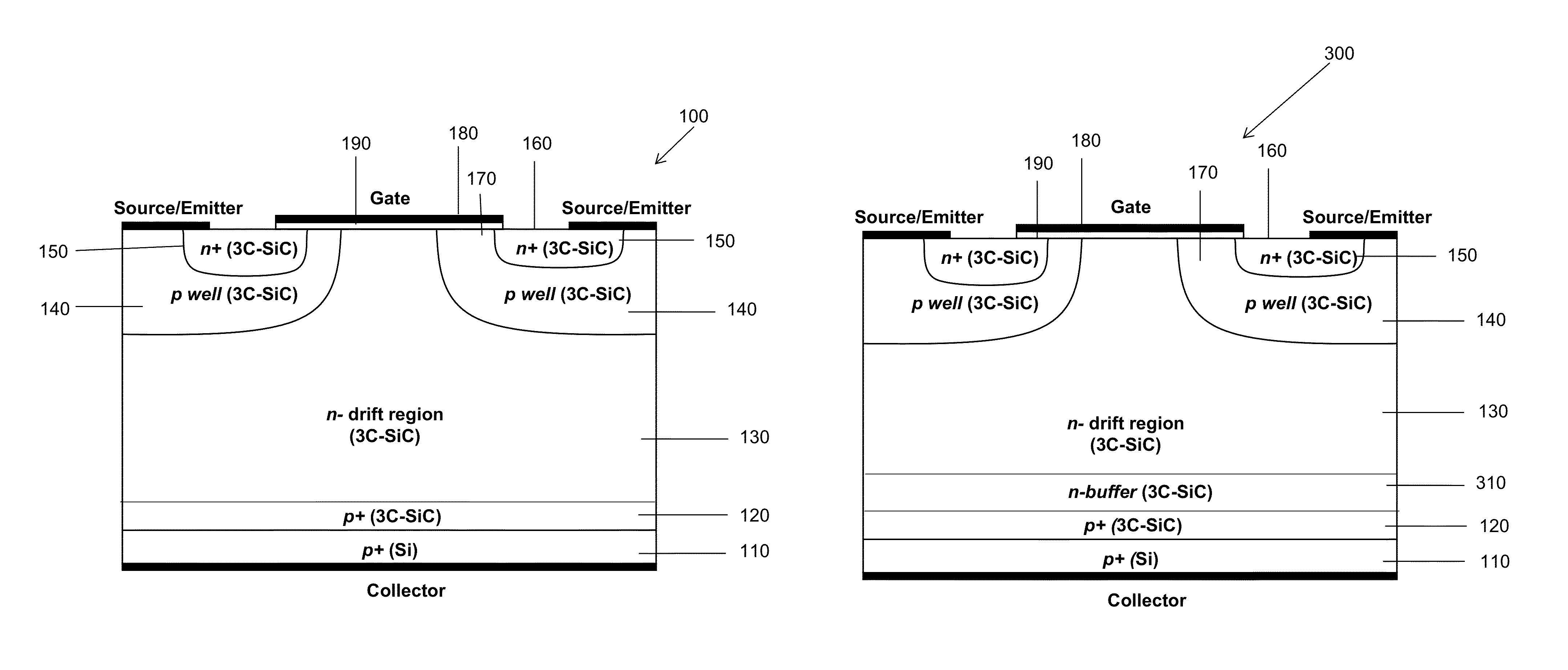
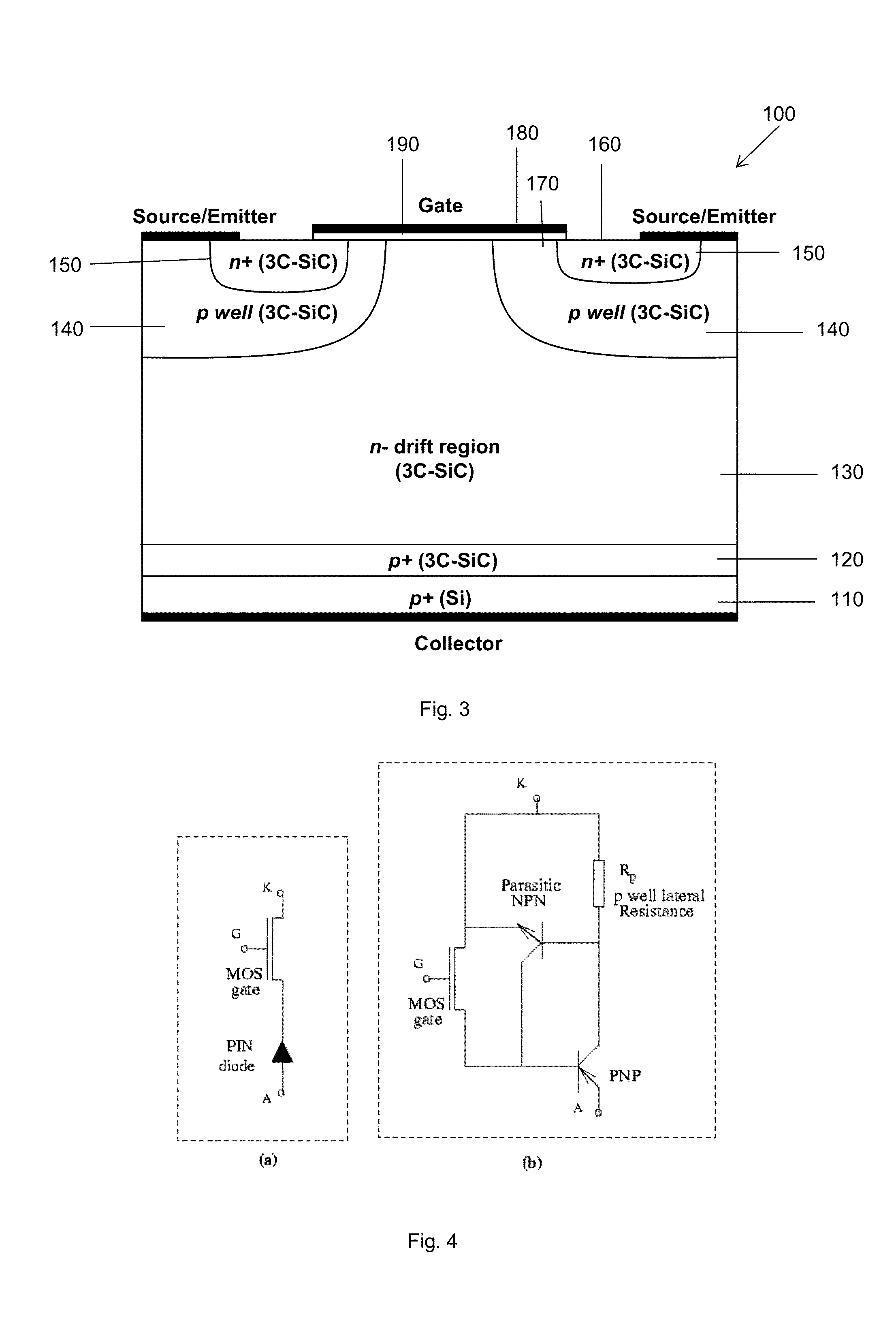
[0041]Referring to FIG. 3, an example of a vertical power semiconductor transistor 100 in the form of an insulated gate bipolar transistor (IGBT) is shown. The transistor 100 has first and second 3-step cubic silicon carbide (3C-SiC) epitaxial layers 120, 130 grown using the process described in WO2013061047 from which the present application claims the continuation in part relationship. The silicon carbide epitaxial layers 120, 130 include a heavily-doped p-type layer 120 which is supported on a p− type silicon substrate 110, and a lightly-doped n-type layer 130 which provides a drift region and which is supported on the p-type silicon carbide layer 120. The first epitaxial layer 120 provides a p-type collector. P-type wells 140 at the surface 160 of the epitaxial layer 130 provide body regions 140. N-type wells 150 within the p-type wells 140 provide contact regions and provide emitters. The body region 140 and the contact region 150 can be formed using 3C-SiC material. A channel ...


PUM


Abstract

A bipolar power semiconductor transistor is disclosed. The transistor includes a semiconductor substrate of a first conductivity type, a first semiconductor region of the first conductivity type disposed on the semiconductor substrate; a semiconductor drift region of a second conductivity type, opposite the first conductivity type, disposed on the first semiconductor region, a body region of the first conductivity type located within the semiconductor drift region, a source region of the second conductivity type located within the body region, a gate placed above and in contact to the source region, the gate to control charge in a channel region between the semiconductor drift region and the source region and to thereby control flow of charge within the semiconductor drift region. The semiconductor substrate includes a material having silicon (Si) and the first semiconductor region includes a material having 3-step cubic silicon carbide (3C-SiC).

Description

RELATIONSHIP TO EARLIER APPLICATIONS[0001]This application is a continuation-in-part of PCT application number PCT / GB2012 / 052627 and published as WO2013 / 061047, which is hereby incorporated by reference in its entirety.FIELD OF THE INVENTION[0002]This invention relates to a power semiconductor transistor, particularly but not exclusively, to a bipolar power semiconductor transistor.BACKGROUND TO THE INVENTION[0003]It is known that semiconductor devices are employed as switches and they operate in “on” and “off” states. In the on-state the device can conduct high currents at modest voltages and the conduction losses are desired to be reduced. In the offstate the device can withstand the system maximum voltage with little or no current passing. There are generally two types of devices in the market, unipolar (MOSFET) where conduction is by majority carriers only, and bipolar where conduction is by majority and minority carriers. One fundamental problem is that to withstand a certain v...

Claims


Application Information

Patent Timeline
Patent Type & Authority Patents(United States)
IPC IPC(8): H01L29/15H01L21/02H01L29/739H01L29/66H01L29/74H01L29/04H01L29/16
CPCH01L29/7393H01L21/0262H01L21/02381H01L21/02447H01L21/02529H01L21/02642H01L21/02645H01L29/045H01L29/1608H01L29/66068H01L29/66363H01L29/7395H01L29/74H01L21/02433H01L21/2015H01L21/3081
Inventor WARD, PETER
Owner ANVIL SEMICON
Why Eureka
Try Eureka