Device for correcting diffraction aberration of electron beam

a technology of electron beam and electron beam, which is applied in the field of substrate manufacturing, can solve the problems of increasing its applicability, unable to obtain the desired resolution of electron beam, and damage to the resist of electron beam, and achieve the effect of suppressing diffraction aberration

Inactive Publication Date: 2015-09-01
HITACHI HIGH-TECH CORP
View PDF11 Cites 4 Cited by
  • Summary
  • Abstract
  • Description
  • Claims
  • Application Information

AI Technical Summary

Benefits of technology

[0023]According to the present invention, in the charged particle beam microscope to observe, measure, and inspect a fine circuit pattern using a charged particle beam, it is possible to suppress the diffraction aberration on the sample by increasing the phase difference within the beam diameter of the vector potential.

Problems solved by technology

However, restrictions on the use represented by the damage to a sample are an obstacle to expanding its applicability.
For example, a critical dimension scanning electron microscope (hereinafter, referred to as a CD-SEM) is an essential measuring apparatus in semiconductor lithography management, but the damage to the resist by the electron beam is an obstacle to measurement.
However, it is not possible to obtain the desired resolution with the electron beam of ultra-low acceleration voltage since optical aberration and a diffraction aberration are increased.

Method used


Image

  • Device for correcting diffraction aberration of electron beam
  • Device for correcting diffraction aberration of electron beam
  • Device for correcting diffraction aberration of electron beam

Examples


first embodiment

[0038]In a first embodiment, an example of application to a scanning electron microscope will be described.

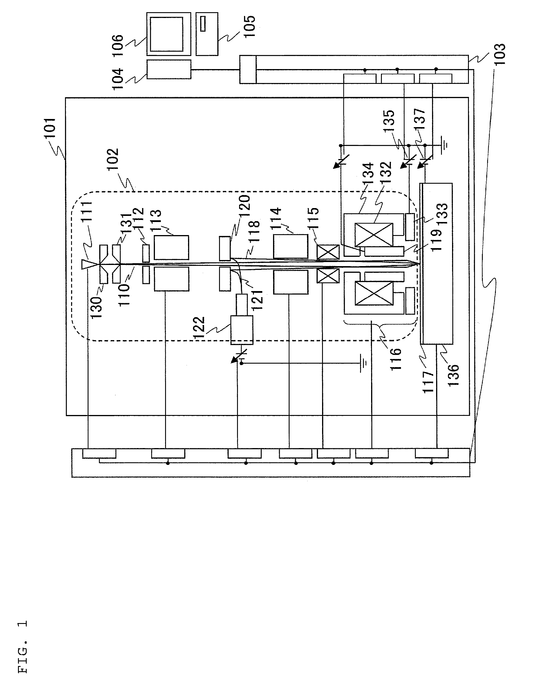
[0039]The scanning electron microscope of the present embodiment is configured to include an electron optical system formed in the vacuum housing, an electron optical system control device disposed around the electron optical system, a host computer that performs overall control of the entire apparatus by controlling each control unit included in a control power supply, a console connected to the control device, and display means including a monitor that displays an acquired image. The electron optical system control device is formed by a power supply unit for supplying a current and a voltage to each component of the electron optical system, a signal control line for transmitting a control signal to each component, and the like. In the present embodiment, the scanning electron microscope is set as an example of an application. However, the present invention may also be applied...

second embodiment

[0047]In a second embodiment, the operation of aberration correction in an example of application to a scanning electron microscope will be described.

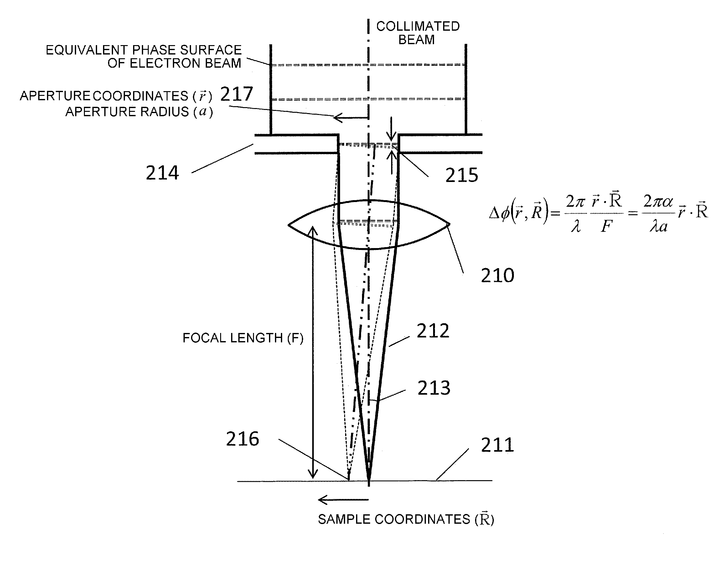
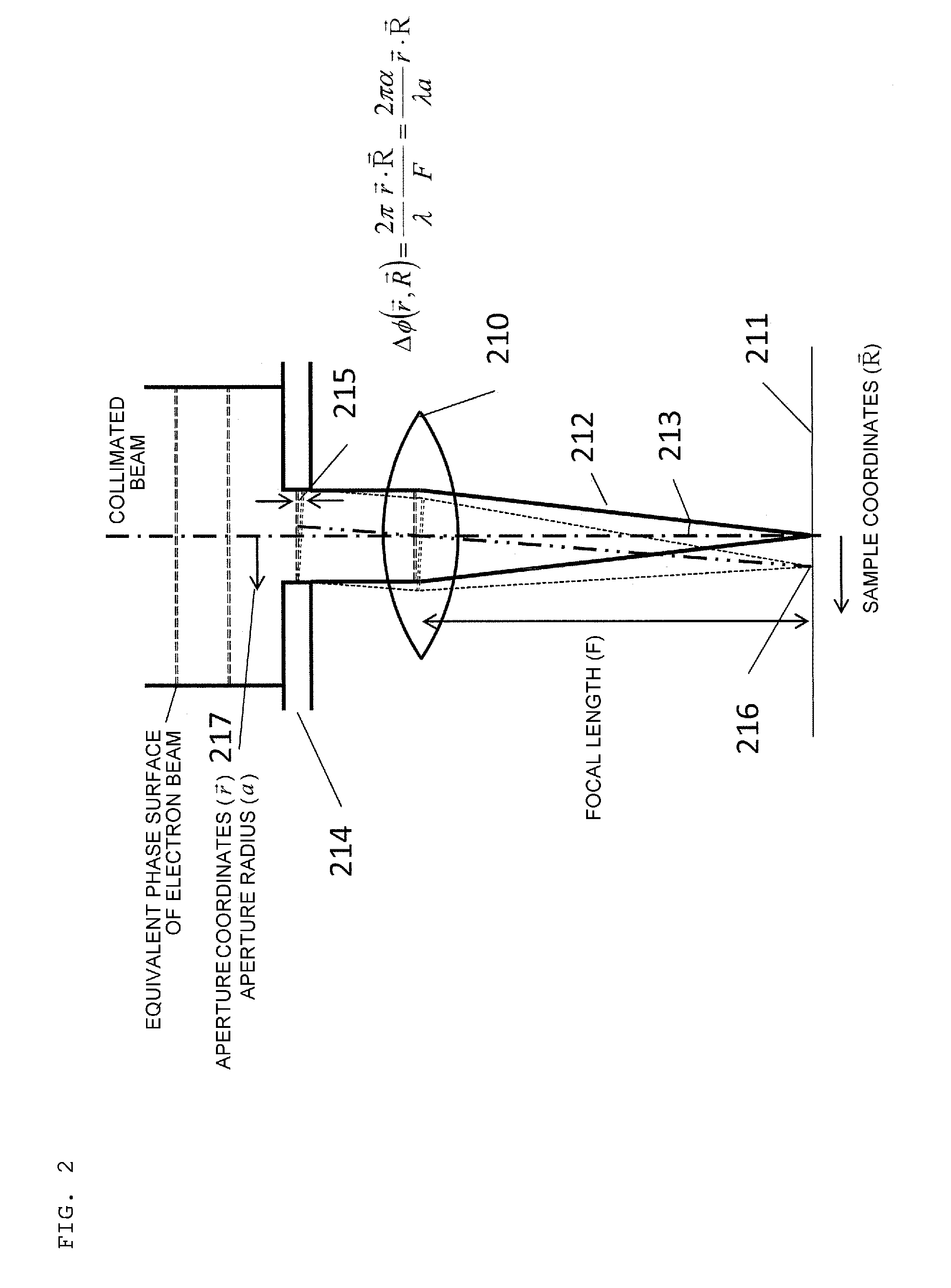
[0048]FIG. 4 is a schematic diagram showing a method of correcting the aberration due to Rayleigh diffraction. Rayleigh diffraction 410 is a phenomenon causing the spot shape expansion of the beam on a sample 409 by interference between a diffracted wave 413 generated on the path of an electron beam 412 up to an objective lens 411 and a diffracted wave 414 generated on the focusing orbit of the electron beam 412 by the objective lens 411.

[0049]Of the Rayleigh diffraction 410, attention is paid to the diffracted wave 413 generated from an objective aperture 415 to the objective lens 411. As a form of the present embodiment, the electron beam 412 from the objective aperture 415 to the objective lens 411 is a collimated beam whose optical orbit is controlled by a condenser lens 416 or the like, and the phase of the electron beam is a plan...

third embodiment

[0052]FIGS. 5A and 5B show a specific method of correcting the Rayleigh diffraction. As described above, a diffraction aberration corrector 510 can induce a vector potential 512 that is parallel to the beam axis of an electron beam 511 and has a symmetrical distribution within the orthogonal plane. An example of the configuration of a scanning electron microscope 515 in which the diffraction aberration corrector 510 is provided will be described below.

[0053]This is the scanning electron microscope 515 including: an electron gun 516; an electron beam 511 emitted from the electron gun 516; a condenser lens 517 that controls the focusing and divergence of the electron beam 511; an objective aperture 513 that limits the beam diameter of the electron beam 511; the diffraction aberration corrector 510 in which a pair 519 of poles of vector potentials formed by a cylindrical pipe to form a solenoid coil in a doughnut-shaped ring 518 or a solenoid coil ring are disposed at the positions of ...


PUM


Abstract

A diffraction aberration corrector formed by the multipole of the solenoid coil ring and having a function of adjusting the degree of orthogonality or axial shift of the vector potential with respect to the beam axis. In order to cause a phase difference, the diffraction aberration corrector that induces a vector potential, which is perpendicular to the beam axis and has a symmetrical distribution within the orthogonal plane with respect to the beam axis, is provided near the objective aperture and the objective lens. A diffracted wave traveling in a state of being inclined from the beam axis passes through the ring of the magnetic flux. Since the phase difference within the beam diameter is increased by the Aharonov-Bohm effect due to the vector potential, the intensity of the electron beam on the sample is suppressed.

Description

TECHNICAL FIELD[0001]The present invention relates to a technique for manufacturing a substrate having a fine circuit pattern, such as a semiconductor device, a liquid crystal, and a magnetic recording medium, and in particular, to a charged particle beam microscope and an inspection method for observing, measuring, and inspecting a fine circuit pattern using a charged particle beam.BACKGROUND ART[0002]With the miniaturization and integration of semiconductor devices, the miniaturization of a circuit pattern is going on in the management or development of the manufacturing process, so that the size of a hole or a groove formed on the wafer is about 10 nm in the case of a fine hole or groove. For this reason, demands for measuring a fine pattern having a size of tens of nanometers with high accuracy and at high speed are increasing more and more. In order to meet the demands of nano-resolution observation that cannot be addressed by the optical microscope, the probe diameter of the e...

Claims


Application Information

Patent Timeline
Patent Type & Authority Patents(United States)
IPC IPC(8): H01J37/14H01J37/153H01J37/10H01J37/147H01J37/26
CPCH01J37/10H01J37/147H01J37/153H01J37/26H01J2237/1534H01J2237/2614
Inventor FUKUDA, MUNEYUKIOSE, YOICHISATO, MITSUGUITO, HIROYUKISUZUKI, HIROSHISUZUKI, NAOMASA
Owner HITACHI HIGH-TECH CORP
Why Eureka
Try Eureka