Check patentability & draft patents in minutes with Patsnap Eureka AI!

Non-volatile memory (NVM) cell and high-K and metal gate transistor integration

a technology of logic transistors and non-volatile memories, applied in the field of integration of non-volatile memories (nvms) with logic transistors, can solve the problems of difficult integration of nvm transistors and logic transistors, and the high k gate dielectrics are typically not able to withstand

Active Publication Date: 2015-09-08
NXP USA INC
View PDF132 Cites 9 Cited by
  • Summary
  • Abstract
  • Description
  • Claims
  • Application Information

AI Technical Summary

Benefits of technology

The patent text describes a method for integrating non-volatile memory (NVM) cells with logic transistors that have high k gate dielectrics and metal gates. The challenge is to integrate these two types of transistors with each other due to their different requirements. The invention provides an integration solution that improves upon previous methods by addressing the issues raised by the integration of NVM cells and logic transistors. The technical effects of the invention include reducing leakage problems for the logic transistors, improving the threshold voltage control of the transistors, and achieving better performance and reliability of the integrated semiconductor structure.

Problems solved by technology

The integration of non-volatile memories (NVMs) with logic transistors has always been a challenge due to the different requirements for the NVM transistors, which store charge, and the logic transistors which are commonly intended for high speed operation.
In any of these cases, the need for this unique layer makes integration of the NVM transistors and the logic transistors difficult.
A further complication is when the logic transistors are high k, metal gate transistors and high voltage transistors.
The high k gate dielectrics typically cannot withstand the high temperatures that are generally best for NVM cells and for high voltage transistors.
Further the high voltage transistors typically have relatively thick layers of oxide for the gate dielectrics that, when etched, can cause a corresponding recess of the isolation oxide exposing the sidewall surface of logic transistor channel regions.
The exposure of the transistor region sidewall surface makes it difficult to control the threshold voltage of the transistors and accordingly makes for a leakage problem for those transistors.

Method used


Image

  • Non-volatile memory (NVM) cell and high-K and metal gate transistor integration
  • Non-volatile memory (NVM) cell and high-K and metal gate transistor integration
  • Non-volatile memory (NVM) cell and high-K and metal gate transistor integration

Examples


Embodiment Construction

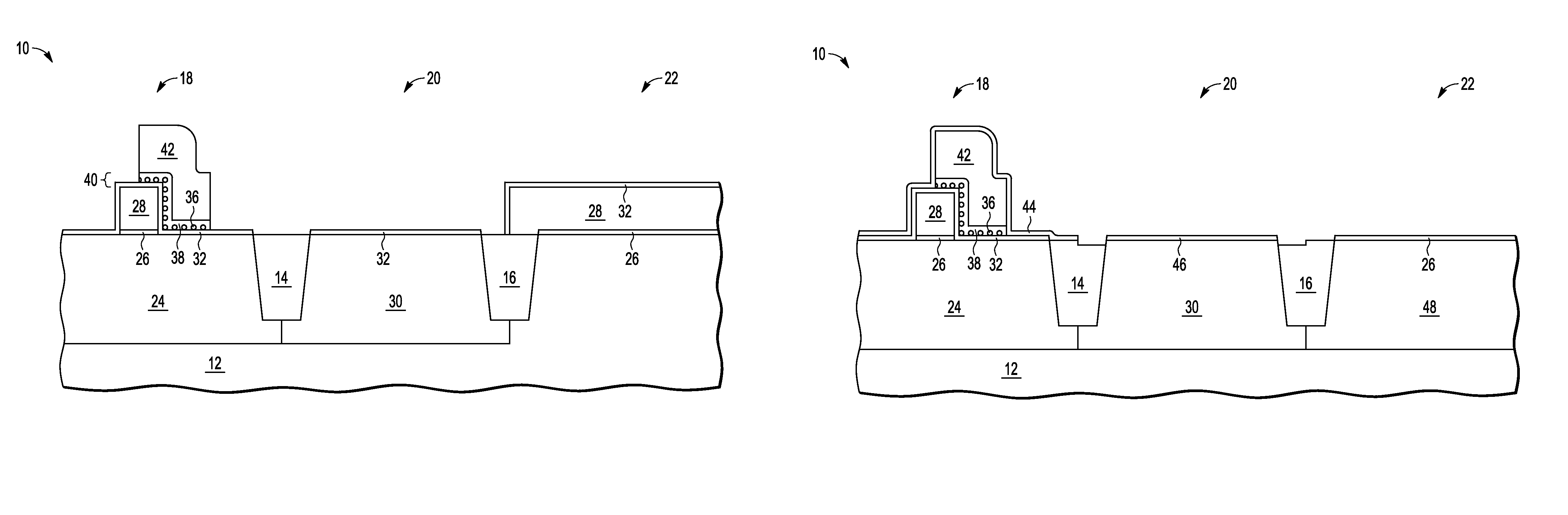
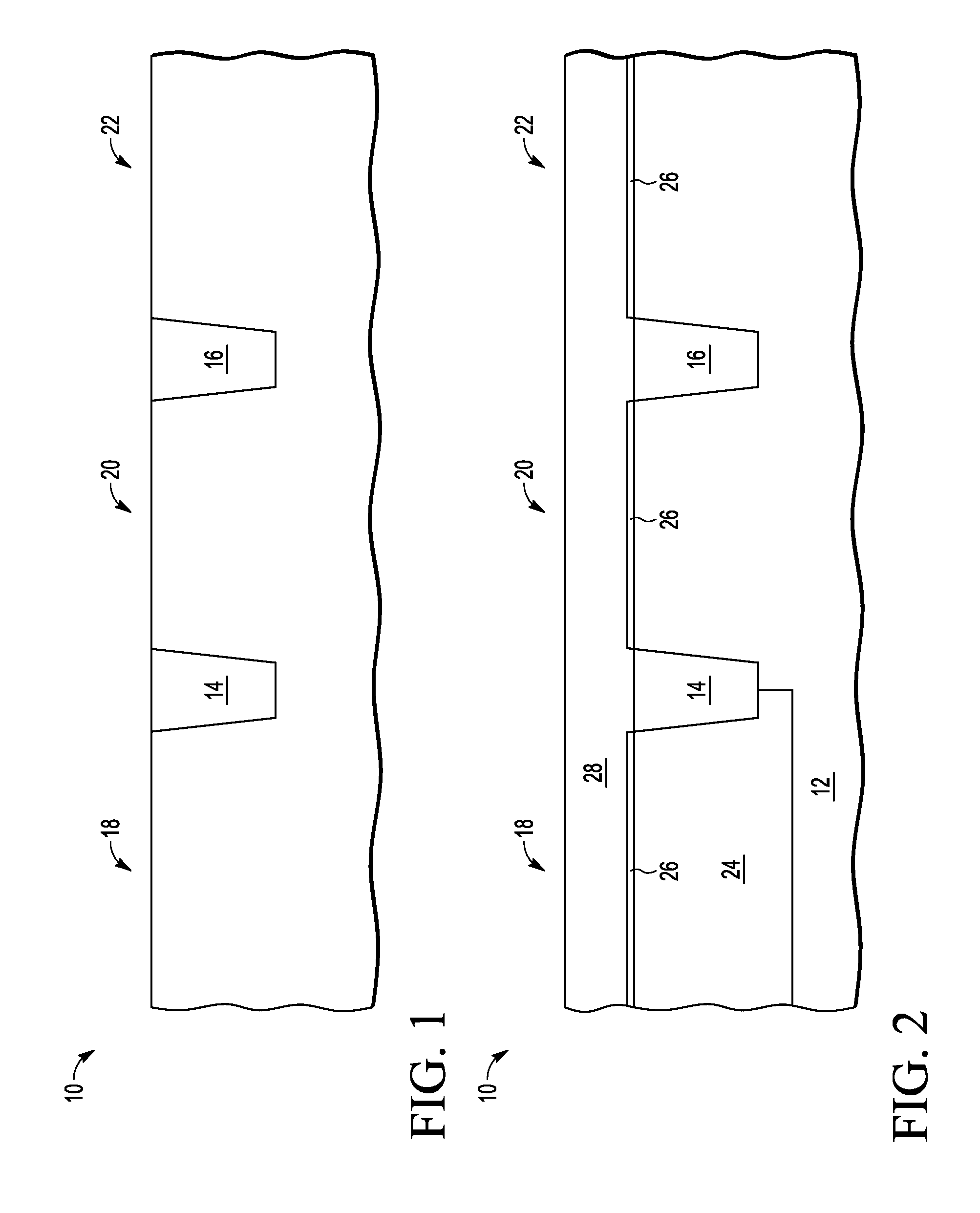
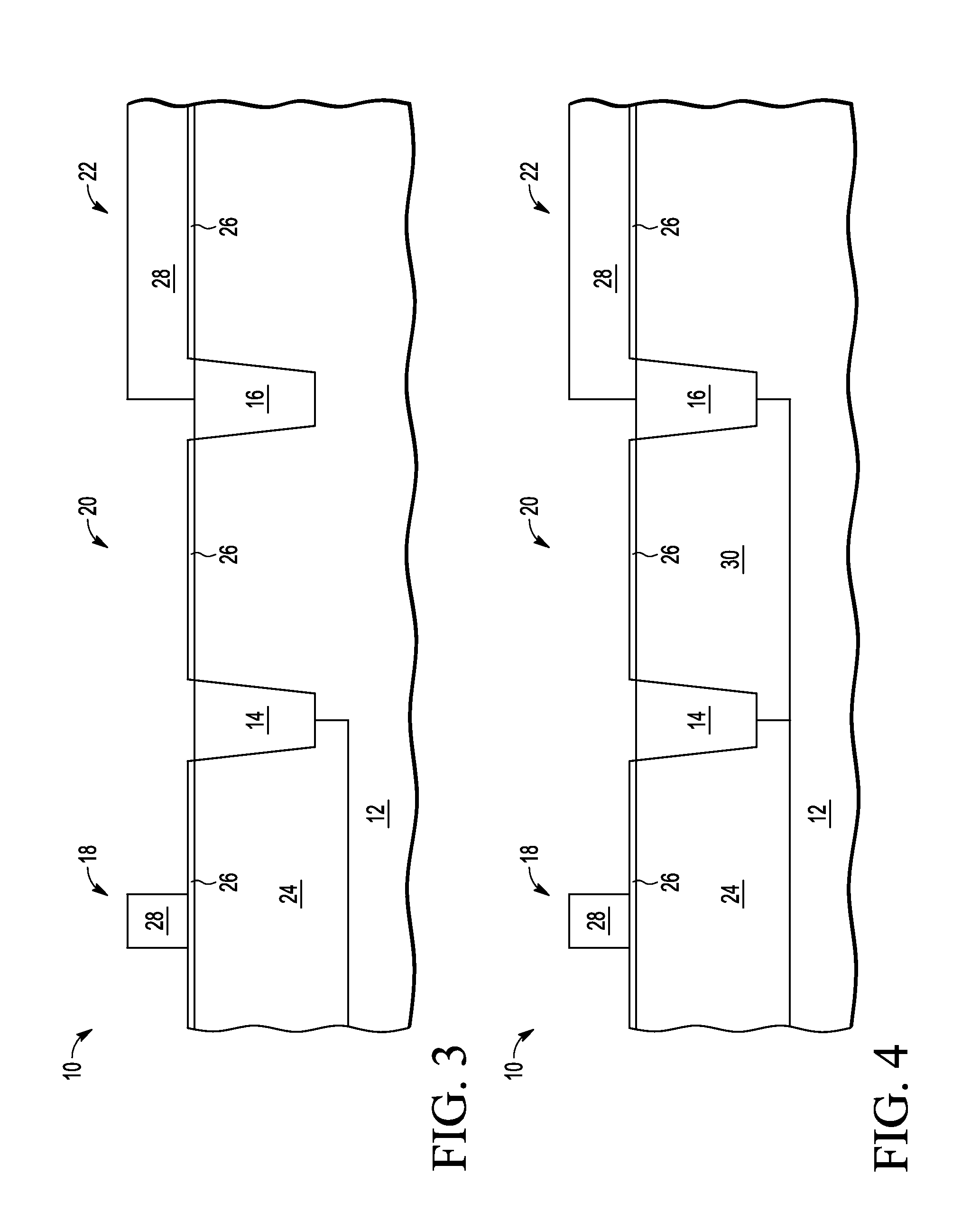
[0033]In one aspect, an integration of a non-volatile memory (NVM) cell in a NVM region of an integrated circuit and a logic transistor in a logic region of the integrated circuit includes forming the gate structure of the NVM cell in the NVM region, including the charge storage layer, while masking the logic region using a polysilicon layer used in forming the select gate in the NVM cell. A well for the logic transistor is not formed until after removing the polysilicon layer from the logic region. This is better understood by reference to the drawings and the following written description.

[0034]The semiconductor substrate described herein can be any semiconductor material or combinations of materials, such as gallium arsenide, silicon germanium, silicon-on-insulator (SOI), silicon, monocrystalline silicon, the like, and combinations of the above. Oxide layer refers to a silicon oxide layer unless otherwise noted. Similarly, nitride layer refers to a silicon nitride layer unless ot...


PUM


Abstract

A method of making a semiconductor device includes depositing a layer of polysilicon in a non-volatile memory (NVM) region and a logic region of a substrate. The layer of polysilicon is patterned into a gate in the NVM region while the layer of polysilicon remains in the logic region. A memory cell is formed including the gate in the NVM region while the layer of polysilicon remains in the logic region. The layer of polysilicon in the logic region is removed and the substrate is implanted to form a well region in the logic region after the memory cell is formed. A layer of gate material is deposited in the logic region. The layer of gate material is patterned into a logic gate in the logic region.

Description

CROSS-REFERENCE TO RELATED APPLICATIONS[0001]This application is related to U.S. patent application Ser. No. 13 / 955,665, filed on Jul. 31, 2013, titled “NON-VOLATILE MEMORY (NVM) AND HIGH-K AND METAL GATE INTEGRATION USING GATE-FIRST METHODOLOGY,” naming Asanga H. Perera as inventor, and assigned to the current assignee hereof.[0002]This application is related to U.S. patent application Ser. No. 13 / 969,180, filed on Aug. 16, 2013, titled “NON-VOLATILE MEMORY (NVM) CELL, HIGH VOLTAGE TRANSISTOR, AND HIGH-K AND METAL GATE TRANSISTOR INTEGRATION,” naming Asanga H. Perera, Cheong M. Hong, and Sung-Taeg Kang as inventors, and assigned to the current assignee hereof.BACKGROUND[0003]1. Field[0004]This disclosure relates generally to non-volatile memory (NVM) cells and other transistor types, and more particularly, integrating NVM cells with logic transistors that have high k gate dielectrics and metal gates.[0005]2. Related Art[0006]The integration of non-volatile memories (NVMs) with logi...

Claims


Application Information

Patent Timeline
Patent Type & Authority Patents(United States)
IPC IPC(8): H01L29/66H01L21/28H01L27/115H10B69/00
CPCH01L29/66833H01L21/28273H01L27/11546H01L29/66825H01L29/66545H01L29/40114H10B41/49
Inventor BAKER, JR., FRANK K.HONG, CHEONG MIN
Owner NXP USA INC
Features
  • R&D
  • Intellectual Property
  • Life Sciences
  • Materials
  • Tech Scout
  • Unparalleled Data Quality
  • Higher Quality Content
  • 60% Fewer Hallucinations
Learn More