Probe and method of manufacture for semiconductor wafer characterization

a technology of semiconductor wafers and manufacturing methods, applied in the field of semiconductor material testing, can solve the problems of poor, consistent probe-wafer contact with repetitive results, affecting conductivity and all related measurement parameters, and the surface of the wafer is typically not perfectly smooth, so as to improve the uniformity of contact with the wafer surface, and improve the spatial density of point contacts

Active Publication Date: 2015-11-03
BRUKER NANO INC
View PDF15 Cites 7 Cited by
  • Summary
  • Abstract
  • Description
  • Claims
  • Application Information

AI Technical Summary

Benefits of technology

[0011]In general, the invention lies in the concept of improving the uniformity of contact between the probe and the underlying wafer surface by adding a new layer of highly conductive material at the tip of the conductive silicone currently used in the most advanced equipment for EL semiconductor material characterization. The idea is to provide a metallic layer suitable for much denser point contact than possible with the flake particles incorporated in the conductive silicone used at the tip of current probes. To that end, a thin layer of very small metallic spheres, preferably made of silver (though, but

Problems solved by technology

Although the method of using conductive probes for semiconductor wafer measurements and tests has been known in the field, the issues of making good, consistent probe-wafer contact with repetitive results are still problematic challenges that vary from application to application.
One major challenge is the precise estimation and consistent repetitiveness of the true contact area between the probe and the surface of the wafer, which affects conductivity and all related measurement parameters.
However, the surface of wafers is typically not perfectly smooth, b

Method used


Image

  • Probe and method of manufacture for semiconductor wafer characterization
  • Probe and method of manufacture for semiconductor wafer characterization
  • Probe and method of manufacture for semiconductor wafer characterization

Examples


Embodiment Construction

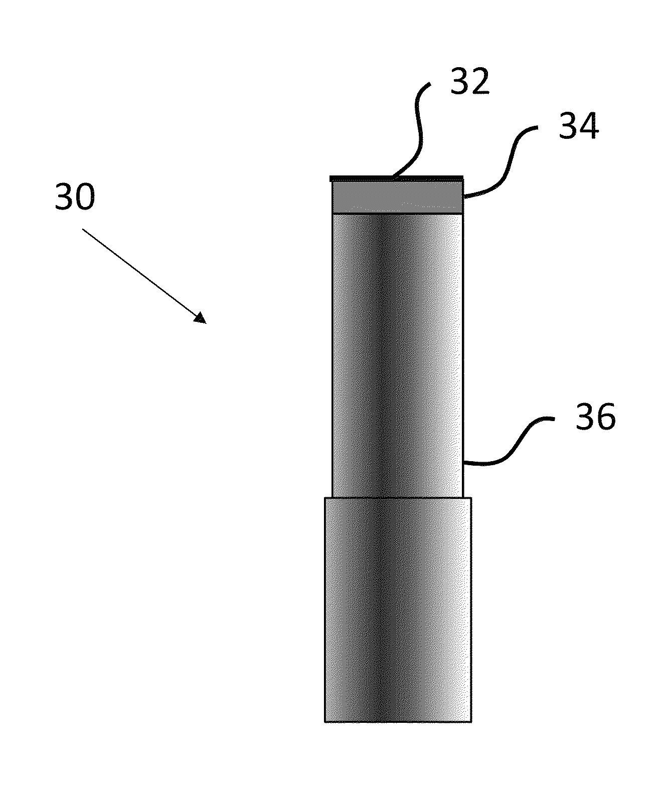
[0030]The invention is a novel conductive probe for characterizing semiconductor materials, in particular electroluminescent (EL) semiconductor wafers in the course of manufacturing light-emitting devices (LEDs). As illustrated in the probe 30 of FIG. 3, the novelty lies in a thin layer 32 of preferably spherical metallic particles of sufficiently small size to ensure a high spatial density of point contacts when the probe engages the surface of the wafer under test. The layer 32 of metallic particles is attached to a thicker layer 34 of cured conductive elastomer, such as silicone, preferably by contacting the metal layer with uncured silicone and then curing it to produce adhesion. The conductive silicone layer 34 is itself similarly attached to a spring-loaded metal pin 36, thereby producing a spring-loaded probe with a metal tip capable of deformation to conform with very high degrees of uniformity and density of point contacts to irregularities in the surface of the wafer under...


PUM


Abstract

A conductive probe for semiconductor material characterization includes a distal metallic layer of micrometer-size particles, an intermediate layer of conformable conductive elastomer material, and a pin attached to the elastomer layer. The probe is preferably manufactured by filling a recess in a bottom plate with the metallic particles, coupling a top plate thereto with a perforation aligned with the recess, and filling the perforation with uncured conductive elastomer. The pin, preferably spring-loaded, is pressed into the perforation to compress the silicone to its intended probe size. The silicone is then allowed to cure at room temperature or in a heated environment, or both.

Description

RELATED APPLICATIONS[0001]This application is a continuation-in-part application of U.S. Ser. No. 13 / 332,657, filed Dec. 21, 2011, which was based on and claimed the priority of U.S. Provisional Application Ser. No. 61 / 525,770, filed Aug. 21, 2011.BACKGROUND OF THE INVENTION[0002]1. Field of the Invention[0003]This invention pertains to the general field of testing of semiconductor materials. In particular, it pertains to an improvement in the probe used for characterizing the properties of electroluminescent semiconductor wafers.[0004]2. Description of the Prior Art[0005]The characterization of semiconductor materials and in particular light-emitting semiconductor structures at the wafer-level (i.e., after forming the p-n junction and the active quantum well layers, but prior to the chip processing steps) is typically carried out with a non-destructive wafer probe. A conductive probe is temporarily placed in contact with the top of the epi-wafer (p-GaN) layer while an electrode con...

Claims


Application Information

Patent Timeline
IPC IPC(8): G01R3/00G01R1/067G01R31/44G01R31/26G01R31/02G09G3/00G01R31/50
CPCG01R1/06761G01R3/00G09G3/006G01R31/44G01R31/2635G01R31/025G01R31/2648G01R31/2656G01R31/50
Inventor CHEN, DONGMUNCH, MARK
Owner BRUKER NANO INC
Why Eureka
Try Eureka