

Graphene sheet, graphene base including the same, and method of preparing the graphene sheet
a graphene base and graphene technology, applied in single-layer graphene, application, bandages, etc., can solve the problems of more difficult to directly form such a graphene sheet on a substrate without transferring graphene, and difficulty in preparing a large-sized graphene sheet with sufficiently few defects, so as to achieve fewer defects, high graphene coverage, and large size
- Summary
- Abstract
- Description
- Claims
- Application Information
AI Technical Summary
Benefits of technology
Problems solved by technology
Method used
Image

Examples
example 1
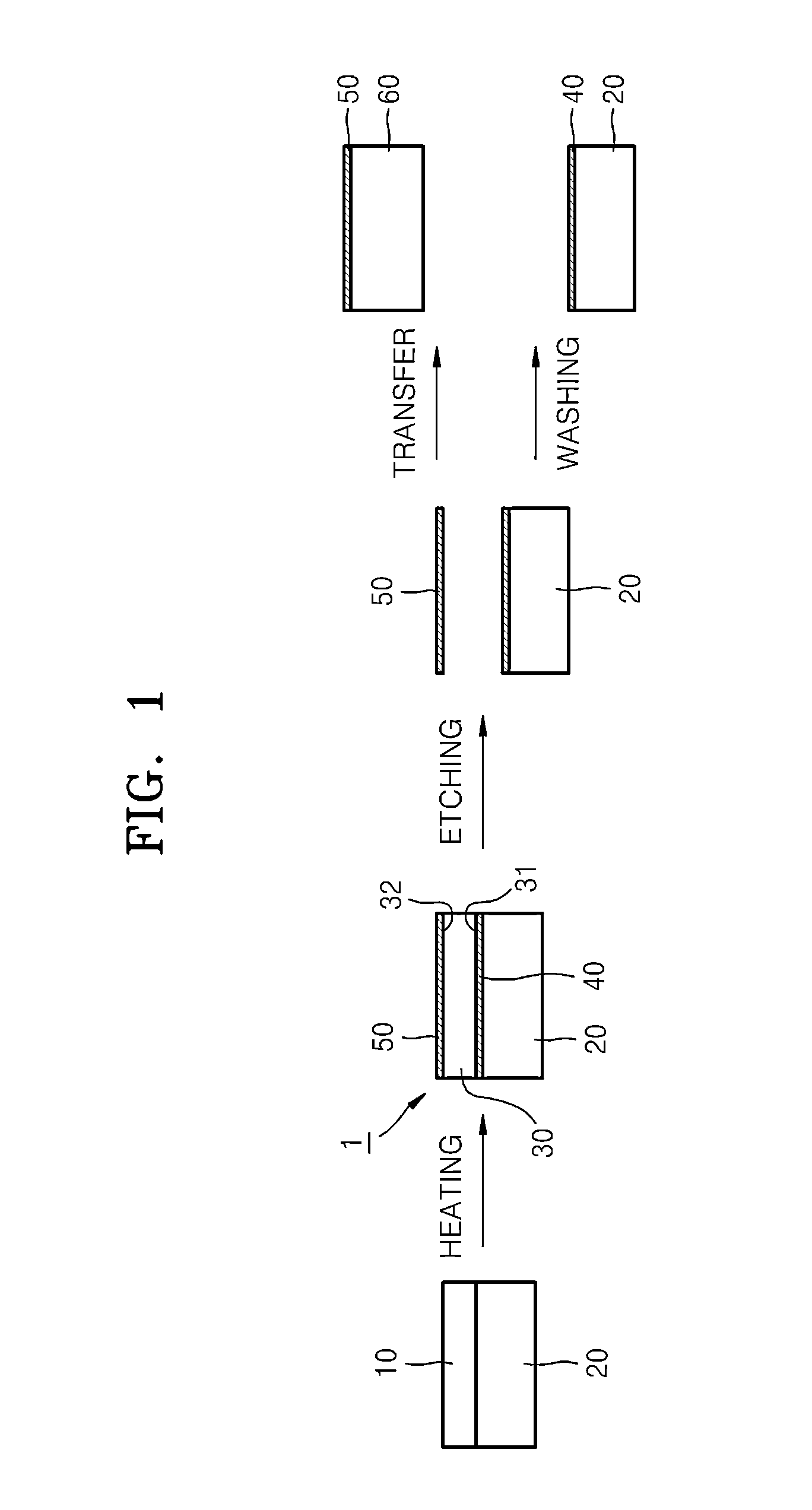
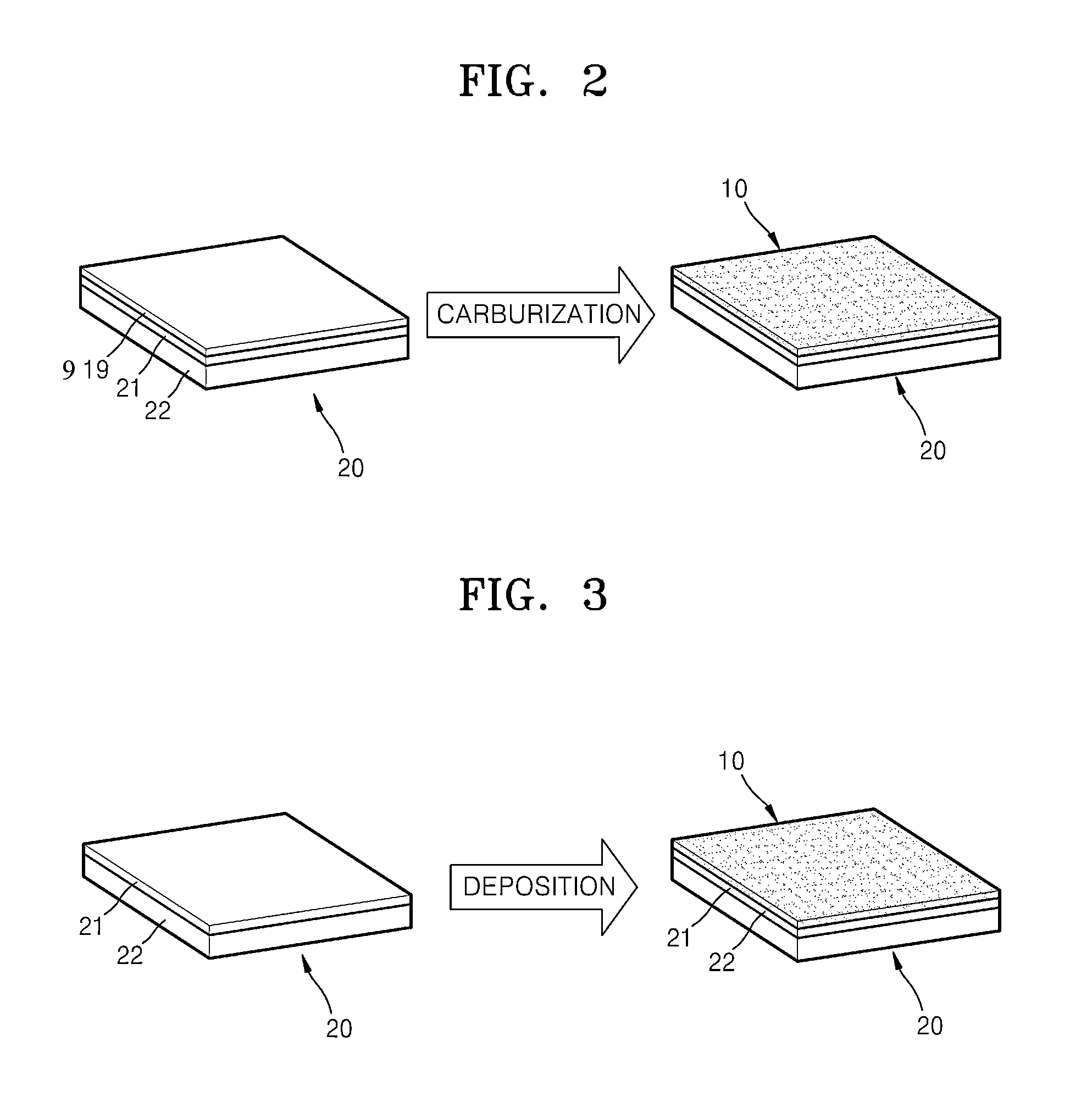
[0101]Nickel was deposited by e-beam evaporation on a 5 centimeter (cm) by 2 cm silicon substrate, which was coated with a 100 nm-thick SiO2 layer, to form a nickel (Ni) layer having a thickness of 300 nm on the silicon substrate.
[0102]The substrate with the Ni layer was immersed in 100 milliliters (mL) of triethylene glycol, maintained at 240° C. for 30 hours, and then cooled. The substrate was removed from the solution and ultrasonically washed with water, ethanol, and then acetone. The substrate was dried, placed in a reaction chamber under an argon atmosphere, heated at a rate of 100° C. per minute to 900° C., maintained at 900° C. for 30 seconds, and then cooled at a rate of 20° C. per minute to form a graphene sheet.
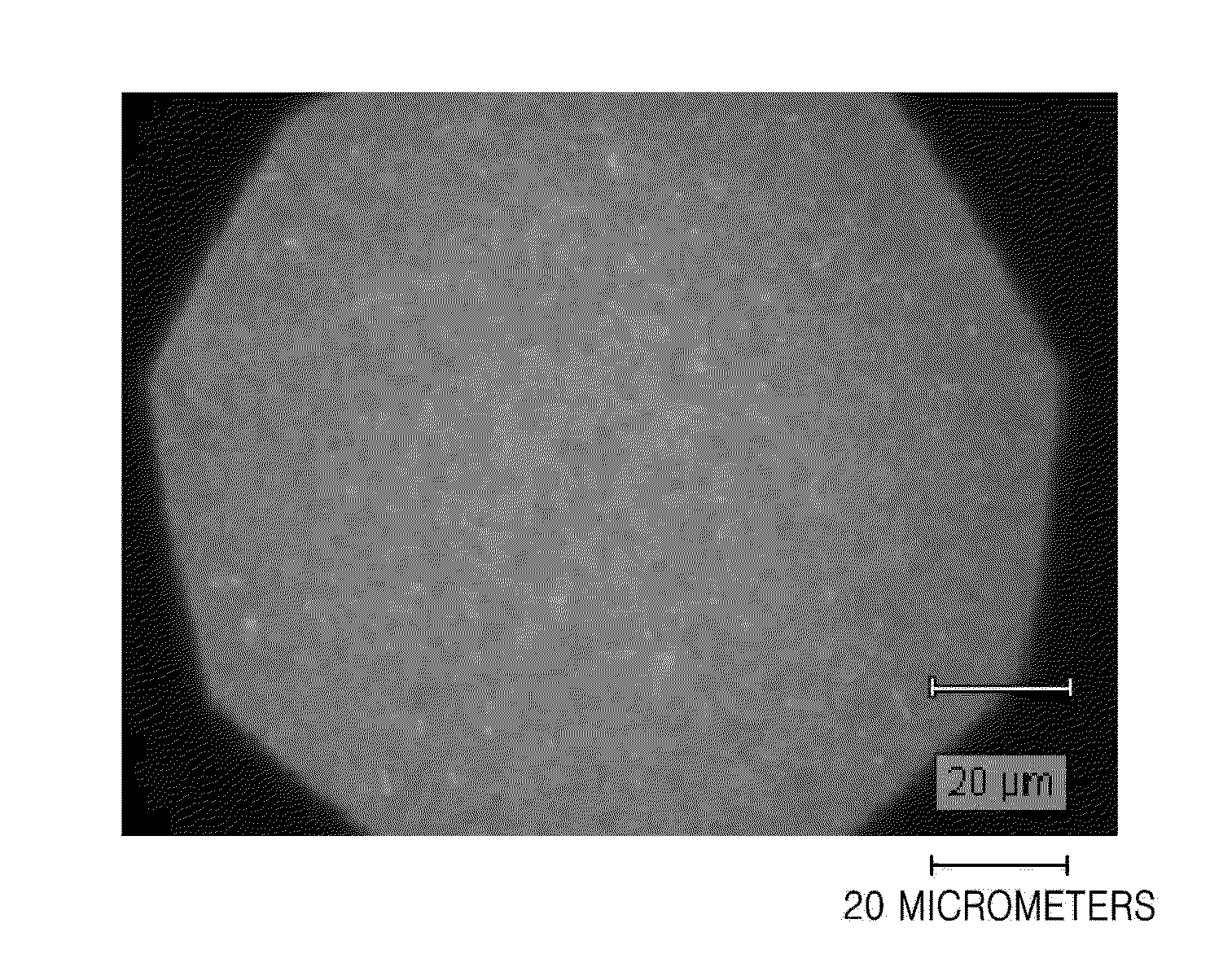
[0103]For analysis purposes, Ni was additionally deposited on the substrate with the graphene sheets to a thickness of about 100 nm and then milled. A cross-section of the resulting structure was analyzed by transmission electron microscopy (“TEM”). The results of ...
example 2
[0107]Nickel was deposited by e-beam evaporation on a 5 cm by 2 cm silicon substrate, which was coated with a 100 nm-thick SiO2 layer 920, to form an Ni layer having a thickness of 200 nm on the silicon substrate. The Ni layer was patterned to provide a predetermined shape by photolithography to have a width of 200 μm in a center region thereof and a width of 30 μm in edge regions thereof.
[0108]The substrate with the patterned Ni layer was immersed in 100 mL of triethylene glycol, maintained at 240° C. for 30 hours and then cooled. The substrate was removed from the solution and ultrasonically washed with water, ethanol, and then acetone. The substrate was dried, placed in a reaction chamber under an argon atmosphere, heated at a rate of 100° C. per minute to 900° C., maintained at 900° C. for 30 seconds, and then cooled at a rate of 20° C. per minute to form patterned graphite sheets.
[0109]The substrate with the graphene sheets was immersed in a Ni etchant solution (TFB, available ...
example 3
[0110]Separate Ni and Cu targets and a mixed gas of acetylene and Ar (1% by volume acetylene in Ar) were sputtered at a power of 700 watts (W) onto a 4″ diameter silicon substrate, which was coated with a 100 nm-thick SiO2 layer, then heated in a H2 atmosphere at 500° C. for 10 minutes, and then heated in an Ar atmosphere at 1000° C. for 30 seconds to provide the substrate with graphene sheets.
[0111]The substrate with the graphene sheets was immersed in a 0.01 M aqueous solution of FeCl3 to remove the Ni / Cu metal layer, removed from the aqueous solution, and then washed with water to recover the graphene sheet grown directly on the substrate. An optical micrograph and a Raman spectrum of the recovered graphene sheet, which had been grown between the substrate and the Ni layer, were obtained. The results are shown in FIGS. 10A and 10B.
[0112]FIG. 10A is an optical micrograph of a 0.01 mm2 area of the graphene sheet. FIG. 10A shows that the imaged area is completely filled with graphen...
PUM
| Property | Measurement | Unit |
|---|---|---|
| area | aaaaa | aaaaa |
| area | aaaaa | aaaaa |
| thickness | aaaaa | aaaaa |
Abstract
Description
Claims
Application Information