Supressing optical loss in nanostructured metals by increasing self-inductance and electron path length

a nano-structured metal and optical loss technology, applied in the direction of basic electric elements, electrical equipment, semiconductor devices, etc., can solve the problems of reducing the efficiency of semiconductor manufacturing, difficult to avoid, and affecting the efficiency of manufacturing, so as to achieve the effect of increasing the fraction of absorption in a semiconductor, increasing the self-inductance of the structure, and reducing the loss

a nano-structured metal and optical loss technology, applied in the direction of basic electric elements, electrical equipment, semiconductor devices, etc., can solve the problems of reducing the efficiency of semiconductor manufacturing, difficult to avoid, and affecting the efficiency of manufacturing, so as to achieve the effect of increasing the fraction of absorption in a semiconductor, increasing the self-inductance of the structure, and reducing the loss

US9246031B1Active Publication Date: 2016-01-26STC UNM

Image

  • Supressing optical loss in nanostructured metals by increasing self-inductance and electron path length
  • Supressing optical loss in nanostructured metals by increasing self-inductance and electron path length
  • Supressing optical loss in nanostructured metals by increasing self-inductance and electron path length

Examples


Embodiment Construction

[0033]This description is not to be taken in a limiting sense, but is made merely for the purpose of illustrating the general principles of the invention. The scope of the invention is defined by the appended claims.

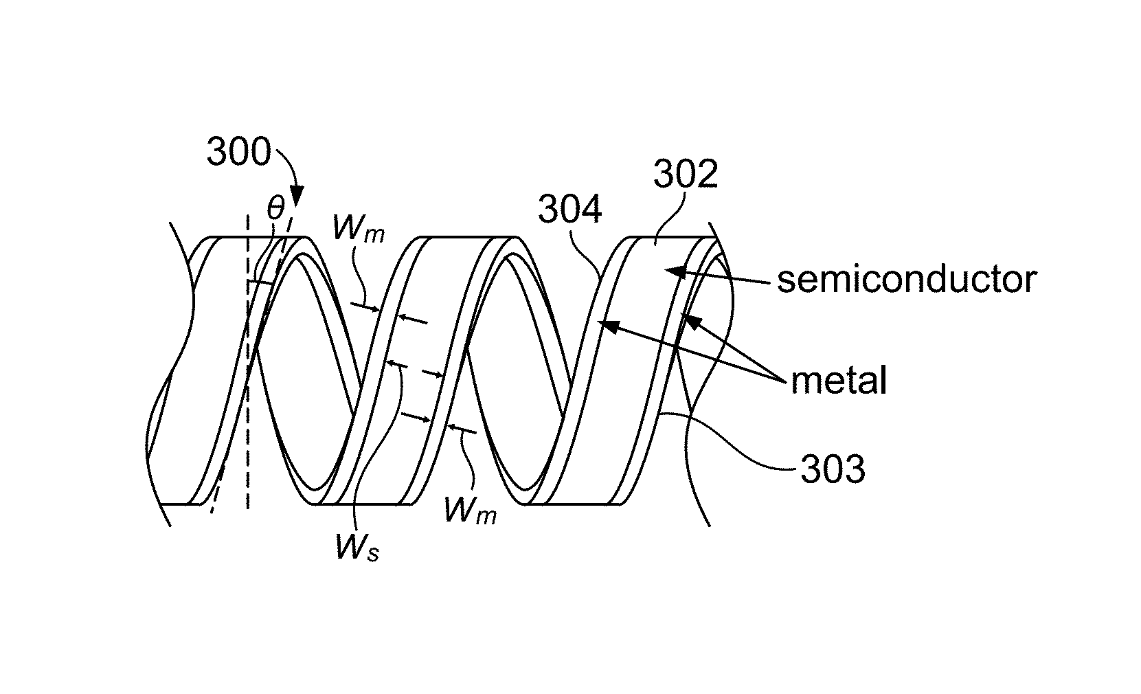
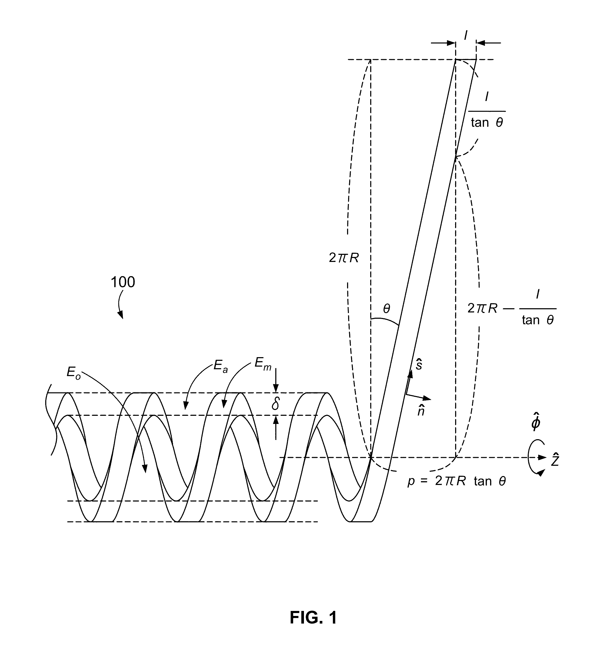
[0034]In one preferred embodiment, the present invention provides an optoelectronic device that decreases absorption in metal nanostructures over a broad band. The invention utilizes the control of self-inductance to hinder the change in the movement of free electrons in metals to increase effective electron mass. For the monolayer array of metal coils 100 shown in FIG. 1, the wire has a rectangular cross section and is helically wound with an outer radius R and a pitch p. These two are related by

p=2πR tan θ,  (1)

[0035]where π / 2−θ is the angle between the wire and the coil axis (z-axis) and θ is assumed to be small so that tan2θ<<1.

[0036]As shown in FIG. 1, the coils form a periodic monolayer array 100 with the distance between the neighboring coil axes equal to α and li...


PUM


Abstract

An optoelectronic device configured to operate at an electromagnetic radiation frequency having metal wire electrodes that are optically transparent as a result of the wires having an effective plasma frequency that is equal to or lower than the electromagnetic frequency at which the device operates. The effective plasma frequency of the wire is lowered by configuring the path of the wire between the terminal ends to be meandering, serpentine, U-shaped and in other non-linear configurations.

Description

RELATED APPLICATIONS[0001]This application claims priority to and the benefit of the filing date of U.S. provisional application Ser. No. 61 / 872,174 filed Aug. 30, 2013 and incorporated herein for all purposes.STATEMENT REGARDING FEDERALLY SPONSORED RESEARCH & DEVELOPMENT[0002]Not applicable.INCORPORATION BY REFERENCE OF MATERIAL SUBMITTED ON A COMPACT DISC[0003]Not applicable.BACKGROUND OF THE INVENTION[0004]Optical absorption in metals is a fundamental loss process, which is difficult to avoid. When metals are nanostructured, the loss is typically more significant as the surface area increases and the structural size becomes comparable to the penetration depth of optical fields. In particular, when surface plasmons—collective oscillations of electromagnetic fields and free electrons in metal surfaces—are excited, energy dissipation can become even greater.[0005]The absorption in metals often limits the efficiency of metal-based nanoscale devices. For example, in optoelectronic dev...

Claims


Application Information

Patent Timeline
26 Jan 2016
Publication
US9246031B1
IPC
H01L21/329; H01L31/0224; H01L31/073; H01L31/0735
CPC
H01L31/022466; H01L31/0735; H01L31/073; H01L31/022433; H01L31/035281; H01L31/0693; Y02E10/543; Y02E10/544
Inventors
HAN, SANG EON; CLARK, SAMUEL