
Kernel masking of DRAM defects

a dram defect and kernel technology, applied in the field of dram defect masking, can solve the problems of increasing cell transistor leakage, increasing cell capacitance, and increasing geometry shrinkage,

Active Publication Date: 2016-03-29
QUALCOMM INC
View PDF16 Cites 42 Cited by
  • Summary
  • Abstract
  • Description
  • Claims
  • Application Information

AI Technical Summary

Problems solved by technology

While denser DRAM chips provide desirable performance and design advantages, the shrinking geometry produces many challenges.
For example, as DRAM process technology continues to scale down, there will be a proportionate decrease in cell capacitance, which increases cell transistor leakage.
In the latter case, wear over the lifetime of the device may lead to an accumulation of errors.
Correcting multiple simultaneous errors on a DRAM requires significant silicon area.
Furthermore, increasing the frequency of refresh adversely impacts the available memory bandwidth and also raises the standby power consumption.

Method used


Image

  • Kernel masking of DRAM defects
  • Kernel masking of DRAM defects
  • Kernel masking of DRAM defects

Examples


Embodiment Construction

[0016]The word“exemplary” is used herein to mean “serving as an example, instance, or illustration.” Any aspect described herein as “exemplary” is not necessarily to be construed as preferred or advantageous over other aspects.

[0017]In this description, the term “application” may also include files having executable content, such as: object code, scripts, byte code, markup language files, and patches. In addition, an “application” referred to herein, may also include files that are not executable in nature, such as documents that may need to be opened or other data files that need to be accessed.

[0018]The term “content” may also include files having executable content, such as: object code, scripts, byte code, markup language files, and patches. In addition, “content” referred to herein, may also include files that are not executable in nature, such as documents that may need to be opened or other data files that need to be accessed.

[0019]As used in this description, the terms “comp...


PUM


Abstract

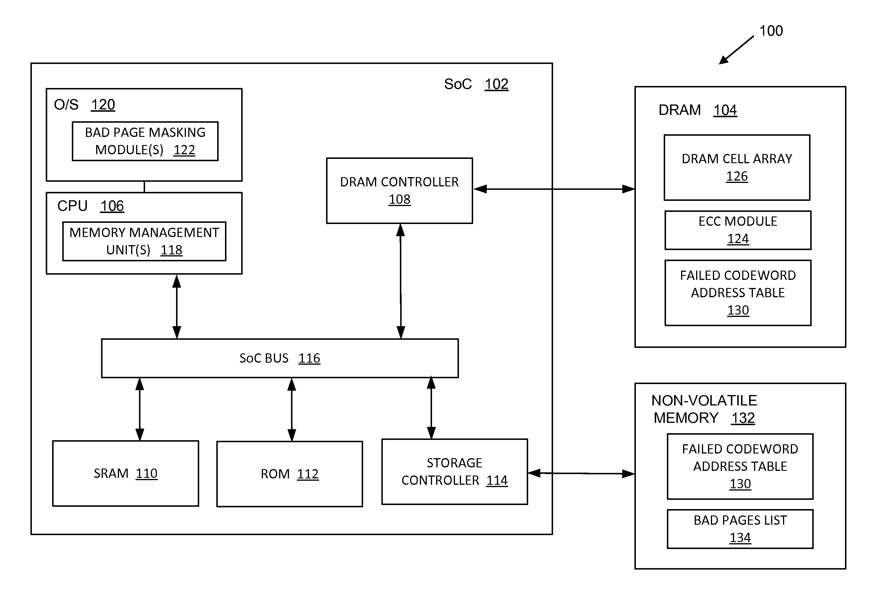
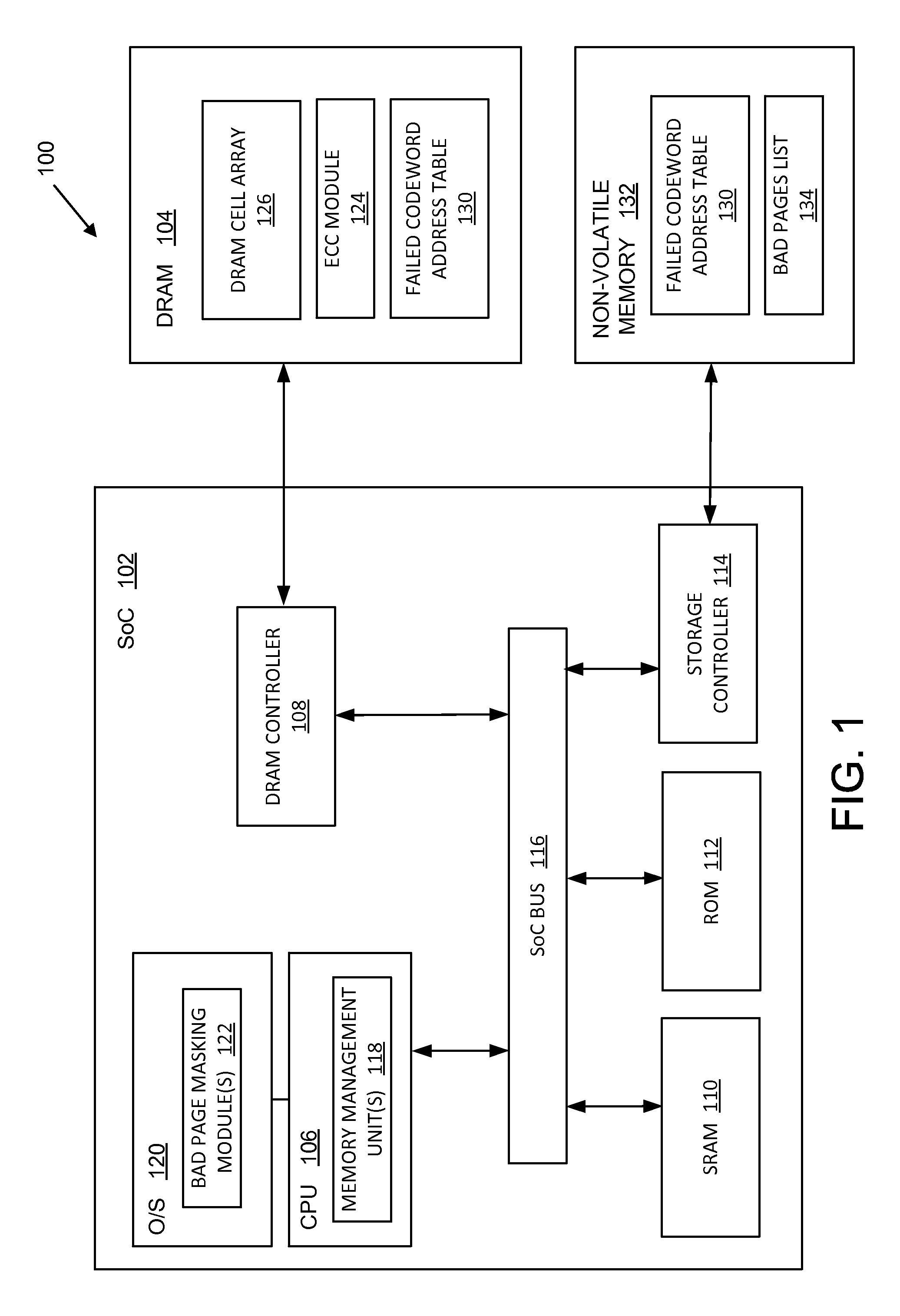
Systems, methods, and computer programs are disclosed for kernel masking dynamic random access memory (DRAM) defects. One such method comprises: detecting and correcting a single-bit error associated with a physical address in a dynamic random access memory (DRAM); receiving error data associated with the physical address from the DRAM; storing the received error data in a failed address table located in a non-volatile memory; and retiring a kernel page corresponding to the physical address if a number of errors associated with the physical address exceeds an error count threshold.

Description

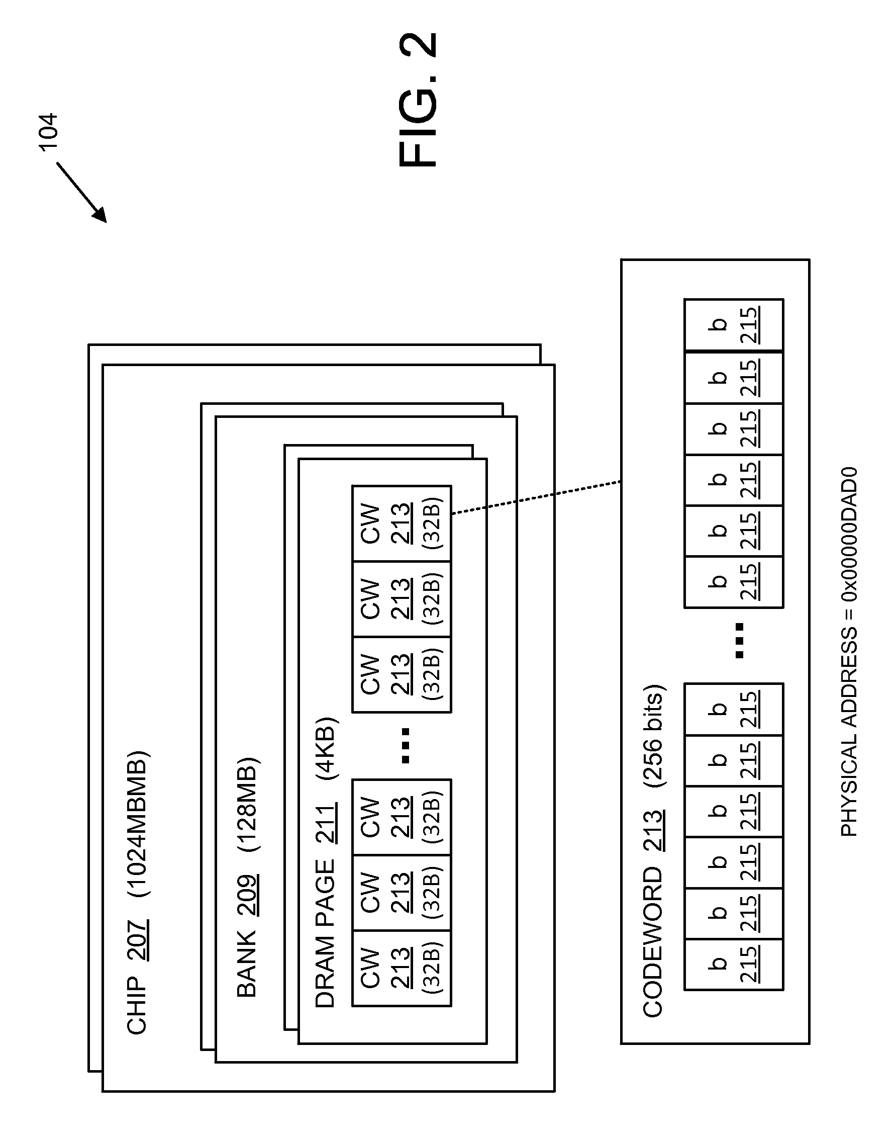
DESCRIPTION OF THE RELATED ART[0001]Dynamic random access memory (DRAM) manufacturing process technology continues to scale down to accommodate increasing demands for greater memory capacity in smaller chips. The common measure of DRAM process technology is half-pitch, which refers to half the distance between cells in a DRAM chip. Current DRAM process technology produces DRAM chips with a half-pitch in the range of 20-30 nanometer (nm), although it is expected that improvements in process technology will scale down to less than 20 nm in the near future.[0002]While denser DRAM chips provide desirable performance and design advantages, the shrinking geometry produces many challenges. For example, as DRAM process technology continues to scale down, there will be a proportionate decrease in cell capacitance, which increases cell transistor leakage. The normal distribution of cell retention across the DRAM die will not tighten, and overall it will continue to exhibit “tails” with some c...

Claims


Application Information

Patent Timeline
Patent Type & Authority Patents(United States)
IPC IPC(8): G11C29/00G06F12/02G11C29/44G06F11/10G06F11/20
CPCG11C29/44G06F11/1048G06F11/1076G06F11/2053G06F12/0246G06F2212/7209G11C2029/4402
Inventor CHUN, DEXTER, T.LI, YANRUDONG, XIANGYUSUH, JUNGWONKIM, JUNG, PILLSRIRAMAGIRI, DEEPTI, VIJAYALAKSHMI
Owner QUALCOMM INC
Learn More