Method for synthesis and formation of a digital hologram for use in microlithography

a microlithography and digital hologram technology, applied in the field of microlithography, can solve the problems of reducing the output rate, and increasing the stepper cost, so as to reduce the deviation from the specified pattern, improve the image contrast, and reduce the noise level of illuminated.

Active Publication Date: 2016-04-12
RAKHOVSKY VADIM
View PDF5 Cites 8 Cited by
  • Summary
  • Abstract
  • Description
  • Claims
  • Application Information

AI Technical Summary

Benefits of technology

[0027]The invention is aimed at obtaining a holographic mask capable of producing an image pattern that contains elements of a sub-wavelength size along with high technological parameters and with reduction of deviations from the specified pattern, improved image contrast, and noise-level reduction in illuminated and non-illuminated areas of the pattern.

Problems solved by technology

The positioning accuracy of the best projection scanning systems (steppers) made by ASML (The Netherlands), which is a leader in the field of microelectronics technology equipment, reaches 10 nm, which is explicitly insufficient for making VLSI ICs with a characteristic element dimension of 20 to 30 nm.
The cost of development when added to the cost of production amounts to hundreds of millions of US dollars.
Projection lenses of modern steppers have reached 600 to 700 mm in diameter, which has caused a rapid increase in stepper cost.
478]] which causes a reduction in output rate and a drastic complication in the focusing system of giant projection lenses and which, again, means higher costs of steppers.
Moreover, the side effects limit using the apertures of such lenses during operation at maximum resolution.
However, experts believe that the cost of such a stepper, even in case of its volume production, would reach 125 million USD, and, according to most optimistic estimates, five to ten years will be required to master the technology of mass production of microprocessors having critical dimensions at a level of 20 nm.
As the monochromatism of used radiation increases, the above-stated effect deteriorates the quality of the received image due to occurrence of diffraction maximums placed at distances of the A order from the center of a projected line.
1. Fundamental difficulties of combining high resolution and considerable depth of focus in one device.
2. Considerable complication in the design and technology of projection devices as the wavelength of radiation used to project an image onto a photoresist becomes shorter.
3. Drastic complication in the optical system and technology of producing a projected object (a mask) as the wavelength used for projection becomes shorter.
5. Extremely low technological flexibility in the production process and very high cost of its modification.
However, the known method of making binary holograms—wherein the image of the transmission areas is produced, for example, by graphical means and then photographed with a significant reduction—does not provide a desired image quality and high resolution primarily because of insufficient accuracy in its production and an insufficient number of transmission areas.
However, the known method of using a hologram to provide an image on the material that is sensitive to used radiation does not allow production of high-quality images due to mutual overlapping of a plurality of diffraction orders, and due to the impossibility of using short-wave radiation sources.
A photographic emulsion having a mirror supported on its reverse side is illuminated by the beam, and interference occurs between this primary illumination and illumination reflected from the mirror, thus creating fringes.

Method used


Image

  • Method for synthesis and formation of a digital hologram for use in microlithography
  • Method for synthesis and formation of a digital hologram for use in microlithography
  • Method for synthesis and formation of a digital hologram for use in microlithography

Examples


Embodiment Construction

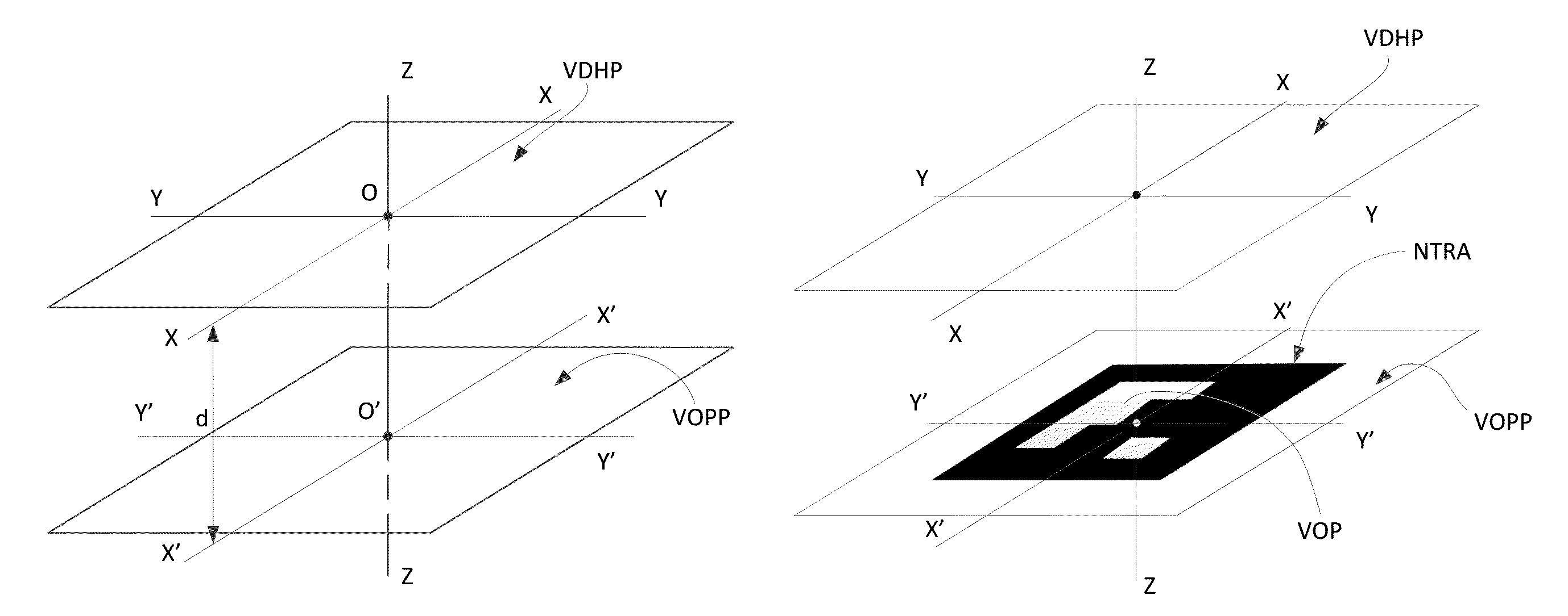
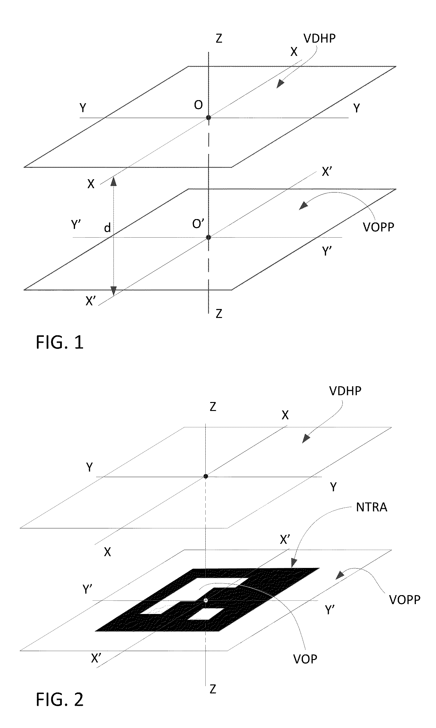
[0045]In the following detailed description, reference will be made to the accompanying drawing(s), in which identical functional elements are designated with like numerals. The aforementioned accompanying drawings show by way of illustration, and not by way of limitation, specific embodiments and implementations consistent with principles of the present invention. These implementations are described in sufficient detail to enable those skilled in the art to practice the invention and it is to be understood that other implementations may be utilized and that structural changes and / or substitutions of various elements may be made without departing from the scope and spirit of present invention. The following detailed description is, therefore, not to be construed in a limited sense.

[0046]In order to understand the principle of the present invention, it is advisable first to more clearly understand and formulate the problem that must be solved by the proposed method. It should be note...


PUM

PropertyMeasurementUnit
operating wavelengthaaaaaaaaaa

Abstract

The invention describes a method of manufacturing a holographic mask capable of producing an image pattern that contains elements of a sub-wavelength size along with decreased deviations from the original pattern. The original pattern is converted into a virtual electromagnetic field and is divided into a set of virtual cells with certain amplitudes and phases, which are mathematically processed for obtaining the virtual digital hologram. The calculation of the latter is based on parameters of the restoration wave, which is used to produce the image pattern from the mask, and on computer optimization by variation of amplitudes and phases of the set of virtual cells and / or parameters of the virtual digital hologram for reaching a satisfactory matching between the produced image pattern and the original pattern. The obtained virtual digital hologram provides physical parameters of the actual digital hologram that is to be manufactured.

Description

BACKGROUND OF THE INVENTION[0001]1. Technical Field[0002]The present invention relates to the semiconductor industry, in particular, to microlithography, and more specifically to a method for synthesizing a holographic photomask used for reconstructing the image recorded on the mask and for subsequently forming the image on the surface of a semiconductor wafer.[0003]2. Description of the Related Art[0004]Lithography and, in particular, photolithography is a well-known technique in semiconductor and printed circuit board (PCB) manufacture for creating electrical components and circuits. Photolithography involves placing a mask in front of a substrate, which has been covered by a layer of photoresist, before exposing both a mask and a substrate to light. The areas of photoresist that are exposed to light react and change chemical properties. The photoresist is then developed in order to remove either the exposed portions of photoresist for a positive resist or the unexposed portions f...

Claims


Application Information

Patent Timeline
Patent Type & Authority Patents(United States)
IPC IPC(8): G03H1/22G03H1/08G03F7/20G03H1/00
CPCG03H1/0808G03F7/70408G03H2001/0094G03H2210/45G03H2260/63
Inventor RAKHOVSKY, VADIMBORISOV, MIKHAILSHAMAEV, ALEKSEYCHELYUBEEV, DMITRYGAVRIKOV, ALEKSANDRCHERNIK, VITALYMIKHEEV, PETER
Owner RAKHOVSKY VADIM
Why Eureka
Try Eureka