Optoelectronic semiconductor chip and method for producing the latter

a technology of optoelectronic semiconductor chips and semiconductor chips, applied in the direction of semiconductor devices, basic electric elements, electrical apparatus, etc., can solve the problems of reducing the efficiency of radiation-emitting semiconductor chips, limiting the brightness per given area and thus radiance, and drastic reduction of effective charge carrier density, so as to avoid ohmic losses in semiconductor chips and high radiance

Active Publication Date: 2016-04-19
OSRAM OLED
View PDF21 Cites 8 Cited by
  • Summary
  • Abstract
  • Description
  • Claims
  • Application Information

AI Technical Summary

Benefits of technology

[0007]Embodiments of the present invention provide an optoelectronic semiconductor chip with which high radiances can be generated, wherein at the same time ohmic losses in the semiconductor chip are avoided. Additional embodiments of the present invention provide a production method for a semiconductor chip improved in this way.
[0010]The semiconductor chip thus comprises two semiconductor layer sequences each with an active zone, wherein the two semiconductor layer sequences share one semiconductor region. The first and second semiconductor layer sequence accordingly comprise a common second semiconductor region of the second conductivity type. Preferably just one semiconductor region of one conductivity type is located between the two active zones of the two semiconductor layer sequences. Overall, the layer stack comprises only exactly three semiconductor regions. As a result of the common semiconductor region, electrical connection of the semiconductor layer sequences may be achieved, for example, by metal contacts. Tunnel junctions between the semiconductor layer sequences or bonding layers are not necessary. The semiconductor chip thus is free of a tunnel junction or bonding layer between the semiconductor layer sequences. At the same time, operation of the semiconductor chip is made possible at low current density. Advantageously the phenomenon of current crowding in the semiconductor chip is reduced due to the low current density. Furthermore, fewer contacts are necessary for optimal current spreading, which results in a preferably simplified epitaxy structure, a reduction in contact surface area, and thus an increase in active surface area.
[0012]Because of the common second semiconductor region, a dielectric mirror without external current spreading can additionally be used advantageously on the n-side of the semiconductor chip. This dielectric mirror is particularly advantageous due to its greater reflectivity than conventional metal mirrors and may further increase efficiency. Current spreading in the layer stack may advantageously proceed on the p-side. In addition, simplified, exact processing is possible with the current spreading layers used.
[0022]According to at least one further embodiment, a surface of the third semiconductor region remote from the second active zone comprises roughening and / or radiation outcoupling structures. Radiation outcoupling from the semiconductor chip preferably proceeds via the roughened or structured surface. The radiation outcoupling structures are preferably three-dimensional structures, for example, pyramids, truncated pyramids and / or lenticular shapes. The roughened surface or the surface provided with radiation outcoupling structures may in particular modify the angle at which the radiation generated in the active zones impinges on the boundary surface between layer stack and surrounding medium, such that this angle differs from the total reflection angle, so advantageously increasing radiation outcoupling efficiency.
[0026]According to at least one further embodiment, a third electrical contact layer is arranged on a surface of the third semiconductor region remote from the second active zone, which third electrical contact layer extends on a side face of the semiconductor chip in electrically insulated manner relative to the semiconductor chip to the second electrical contact layer and electrically contacts the third semiconductor region. The second electrical contact layer and the third electrical contact layer are preferably not electrically insulated from one another, but rather are in electrical contact with one another. The third electrical contact layer is preferably transparent to radiation emitted by the active zones, being, for example, a TCO (Transparent Conductive Oxide) layer. In this way, efficient radiation outcoupling may also be ensured on the third semiconductor region side.

Problems solved by technology

The drop in the efficiency of radiation-emitting semiconductor chips as current density increases has been a long-term problem, which, inter alia, limits brightness per given area and thus radiance.
This leads to a drastic reduction in effective charge carrier density and to ohmic losses, for example, at tunnel junctions, which can be integrated into the semiconductor chip.
However, these vertically stacked semiconductor chips display an elevated operating voltage, since ohmic losses at the tunnel junction cannot be avoided.
In addition, radiation efficiency is impaired by internal absorption in the semiconductor chip, even if the tunnel junction is operated in a loss-free manner.

Method used


Image

  • Optoelectronic semiconductor chip and method for producing the latter
  • Optoelectronic semiconductor chip and method for producing the latter
  • Optoelectronic semiconductor chip and method for producing the latter

Examples


Embodiment Construction

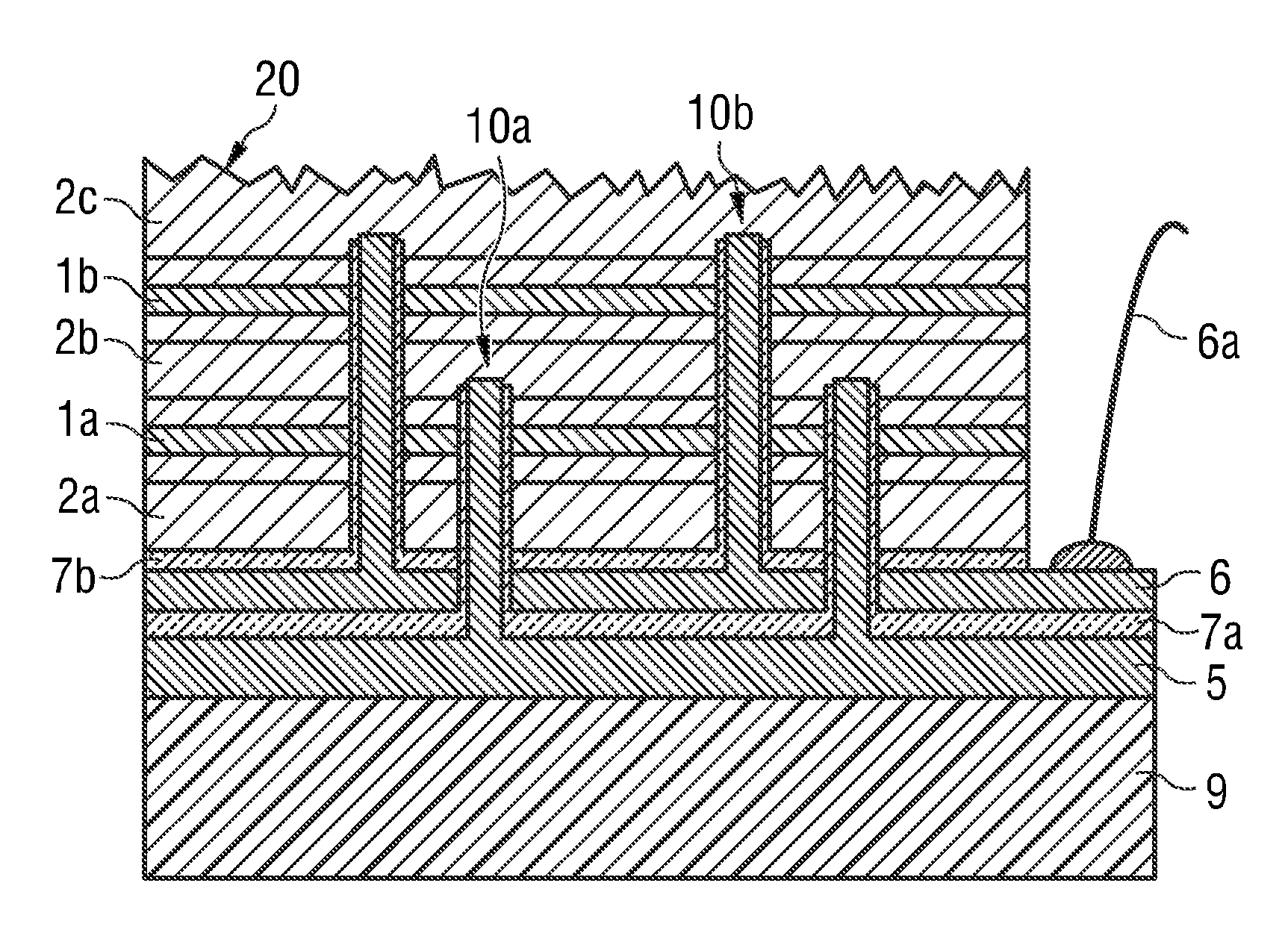
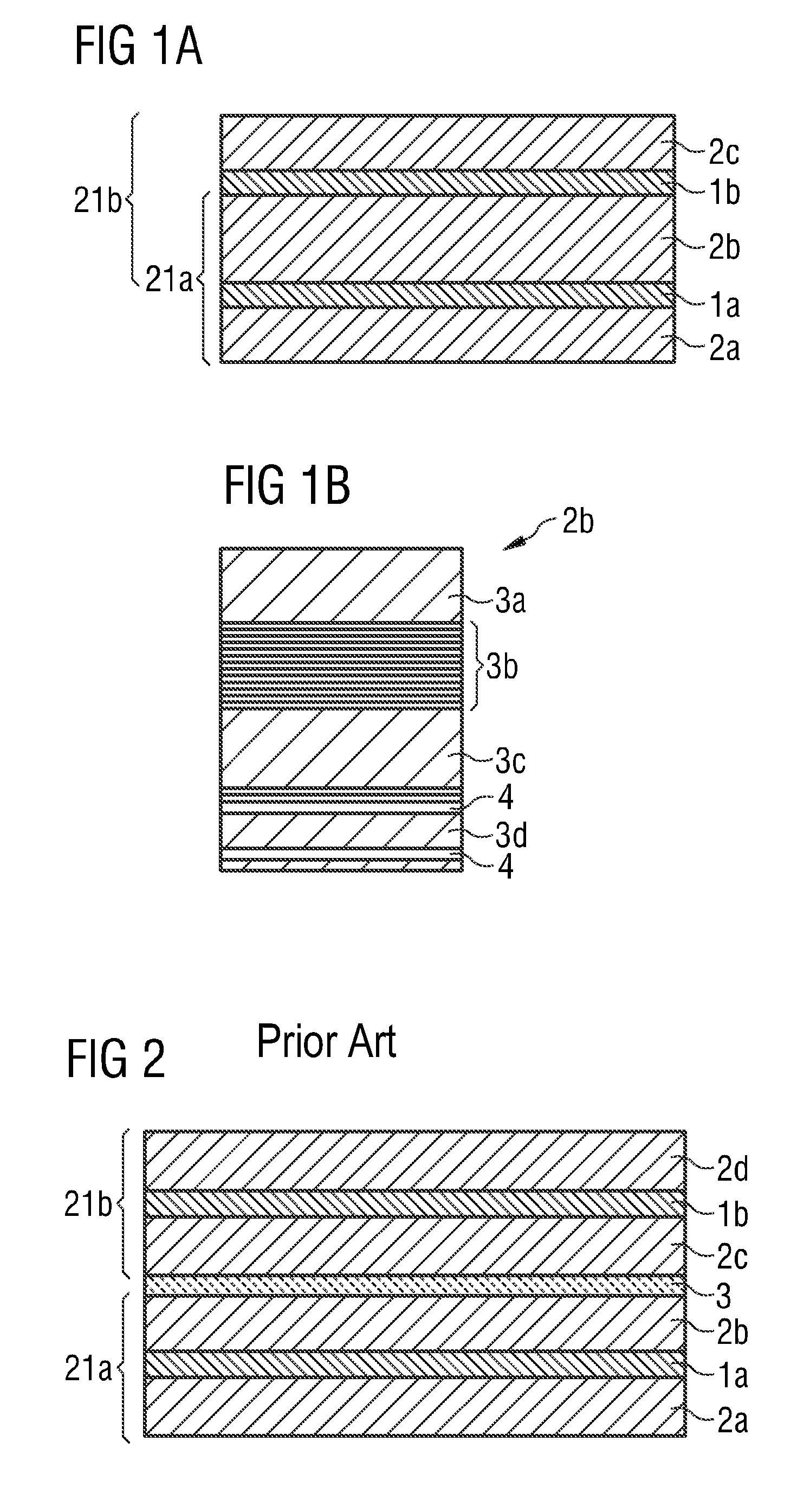
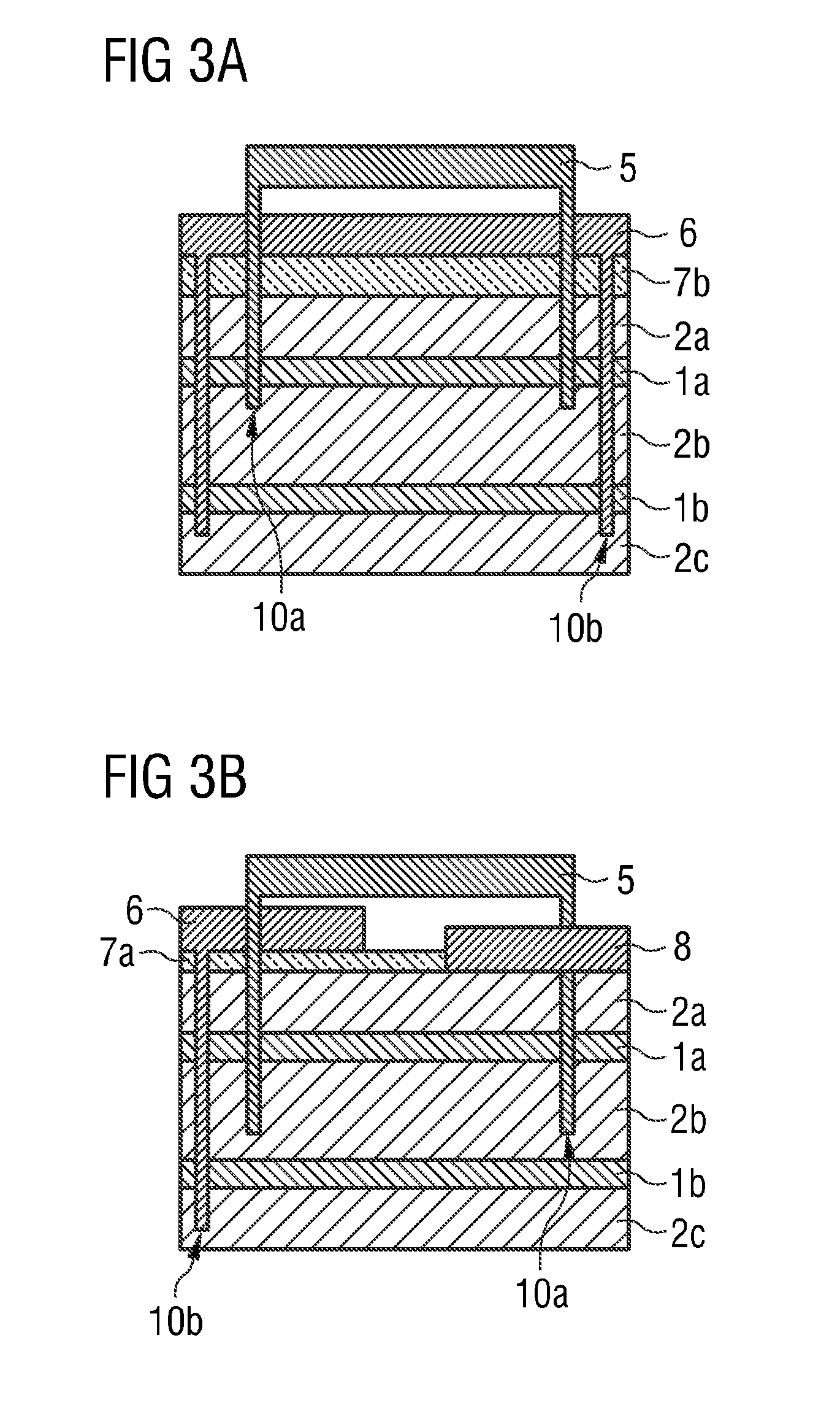
[0043]In the figures, identical or identically acting components may in each case be provided with the same reference numerals. The components illustrated and their size ratios to one another should not be viewed as being to scale. Rather, individual elements such as for example layers, structures, components and regions can be shown exaggeratedly thick or large for greater ease of depiction and / or better comprehension.

[0044]FIG. 2 shows a cross-section of a semiconductor chip with a layer stack according to the prior art. The semiconductor chip comprises a first semiconductor layer sequence 21a and a second semiconductor layer sequence 21b. The first semiconductor layer sequence 21a comprises a first semiconductor region 2a of a first conductivity type, a second semiconductor region 2b of a second conductivity type and a first active zone 1a arranged between the first semiconductor region 2a and the second semiconductor region 2b for generating a first electromagnetic radiation. Th...


PUM


Abstract

A semiconductor chip with a layer stack includes a first semiconductor layer sequence and a second semiconductor layer sequence. The first semiconductor layer sequence includes a first semiconductor region of a first conductivity type, a second semiconductor region of a second conductivity type and an active zone arranged therebetween. The second semiconductor layer sequence includes the second semiconductor region of the second conductivity type, a third semiconductor region of the first conductivity type and a second active zone arranged therebetween.

Description

[0001]This patent application is a national phase filing under section 371 of PCT / EP2012 / 069868, filed Oct. 8, 2012, which claims the priority of German patent application 10 2011 116 232.5, filed Oct. 17, 2011, each of which is incorporated herein by reference in its entirety.TECHNICAL FIELD[0002]The invention relates to an optoelectronic semiconductor chip with a first semiconductor layer sequence and a second semiconductor layer sequence. The present invention further relates to a method for producing such a semiconductor chip.BACKGROUND[0003]The drop in the efficiency of radiation-emitting semiconductor chips as current density increases has been a long-term problem, which, inter alia, limits brightness per given area and thus radiance. Semiconductor chips connected in series and / or stacked on one another may solve this problem in part. With semiconductor chips grown monolithically over one another and which emit radiation in the visible wavelength range, the large band gap resu...

Claims


Application Information

Patent Timeline
Patent Type & Authority Patents(United States)
IPC IPC(8): H01L29/18H01L33/00H01L27/15H01L33/08H01L33/38H01L33/62H01L33/30H01L33/06
CPCH01L33/06H01L27/15H01L33/005H01L33/08H01L33/382H01L2224/48463
Inventor AVRAMESCU, ADRIAN STEFANRODE, PATRICKSTRASSBURG, MARTIN
Owner OSRAM OLED
Why Eureka
Try Eureka