
Bonding structure of bonding wire

a technology of bonding wire and bonding structure, which is applied in the direction of solventing apparatus, manufacturing tools, transportation and packaging, etc., can solve the problems of short storage life, material cost, and performance degradation of copper bonding wire, so as to improve the continuous operability of bonding, increase the bonding strength, and strengthen the bonding strength

Active Publication Date: 2016-05-03
NIPPON MICROMETAL CO LTD
View PDF19 Cites 2 Cited by
  • Summary
  • Abstract
  • Description
  • Claims
  • Application Information

AI Technical Summary

Benefits of technology

[0053]The bonding structure of the bonding wire according to the present invention can provide the enhanced bonding strength in the reverse bonding connection using the copper-based bonding wire by inhibiting non-stick failures and peeling failures at the bonding part between the stud bump and the bonding wire to improve the continuous operability of bonding and to increase the bonding strength. Also, the bonding strength of the bonding part between the stud bump and the electrode can be improved. In addition, reliability in a high-temperature environment during the operation can be improved. To mention in more detail, the life of the bonding can be prolonged in each of a heat cycle test, heat impact test, high-temperature and high-humidity test, high-temperature and high-humidity bias test and high-temperature heating test. Also, the loop shape can be stabilized.
[0054]As a result, the operability and the productivity can be improved and the bonding reliability can also be improved in the reverse bonding connection using the copper-based bonding wire using inexpensive materials. It is possible to connect using the copper-based bonding wire in a packaging structure (stacked packaging) having a laminate structure obtained by stacking semiconductor chips and the multi-chip packaging, which are semiconductor packaging structures using the reverse bonding connection in many cases.

Problems solved by technology

However, it is desired to use other types of metal with lower material cost for the bonding wire because gold is expensive.
The performance of the copper bonding wire is deteriorated by oxidation of the surface of the wire, and therefore a shorter storage life is concerned.
Moreover, in applications such as LSIs using thinner wires having a wire diameter of 25 μm or less, though the evaluation of the wire has been started, the copper-based bonding wire has not been put to practical use.
This leads to demand stricter requirements for wire connection.
In the reverse bonding, there is a risk of occurring defects than in the case of the forward bonding because two bonding operations, the electrode / bump bonding and the bump / wedge bonding are carried out.
There has actually been no substantial report concerning practical use of the copper-based bonding wire in the reverse bonding so far.
However, there is a fear that, as is evident from the fact that no copper-based bonding wire has been used for the reverse bonding, it may be difficult to practically use the bump / wedge bonding using the copper-based bonding wire.

Method used


Image

  • Bonding structure of bonding wire
  • Bonding structure of bonding wire
  • Bonding structure of bonding wire

Examples


examples

[0112]The present invention will be described in detail by way of examples.

[0113]For cupper as the raw material of the bonding wire, a high purity material having a purity of about 99.99 wt % or more was used, and an alloy having an appropriate amount of P, B, Zr, Bi, La and the like added thereto as alloy elements according to the need was melted to produce an ingot. A raw material having a purity of 99.99 wt % or more was prepared as each material of Pd, Au, Pt and Ag for an outer skin layer. In the case of a monolayer copper wire, predetermined alloy elements were added and melted to produce an ingot. In the manufacturing of a multilayer copper wire, a high-purity copper wire or copper alloy wire narrowed to a certain wire diameter was prepared as a core material in advance, and the electrolytic plating method, the electroless plating method, the vapor deposition method, the fusion method or the like was conducted in order to form an outer skin layer made of a different metal on ...


PUM


Abstract

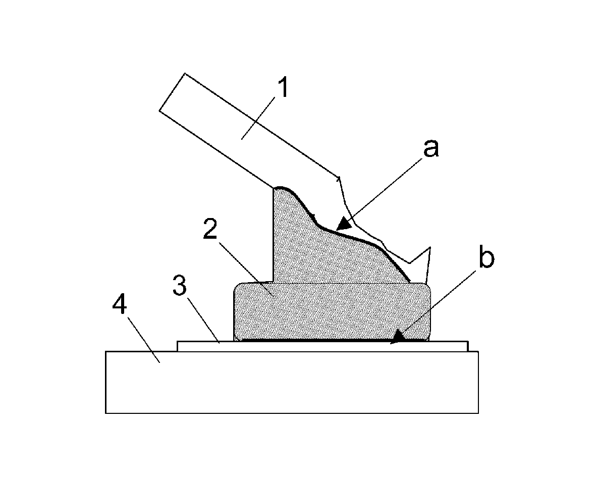
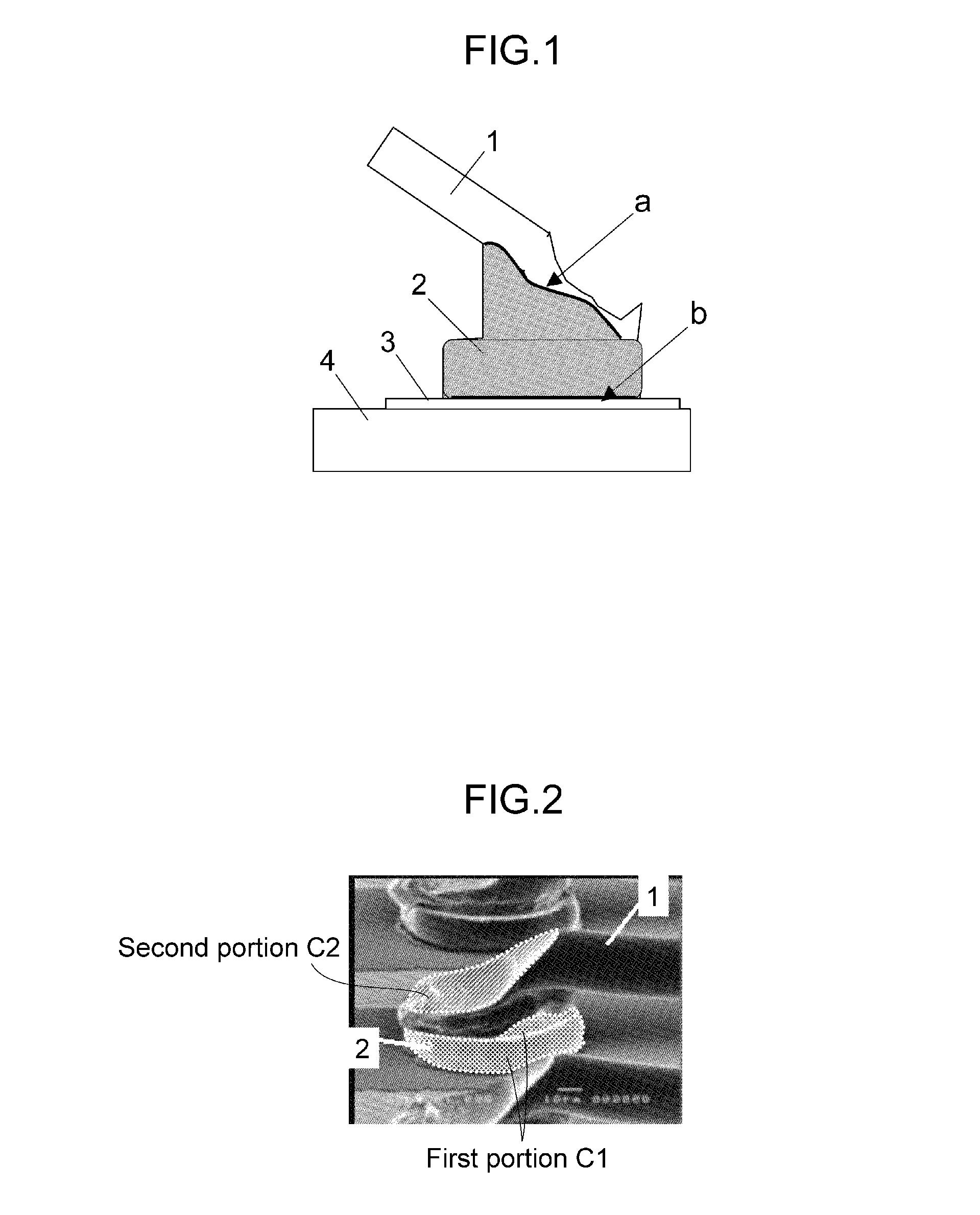
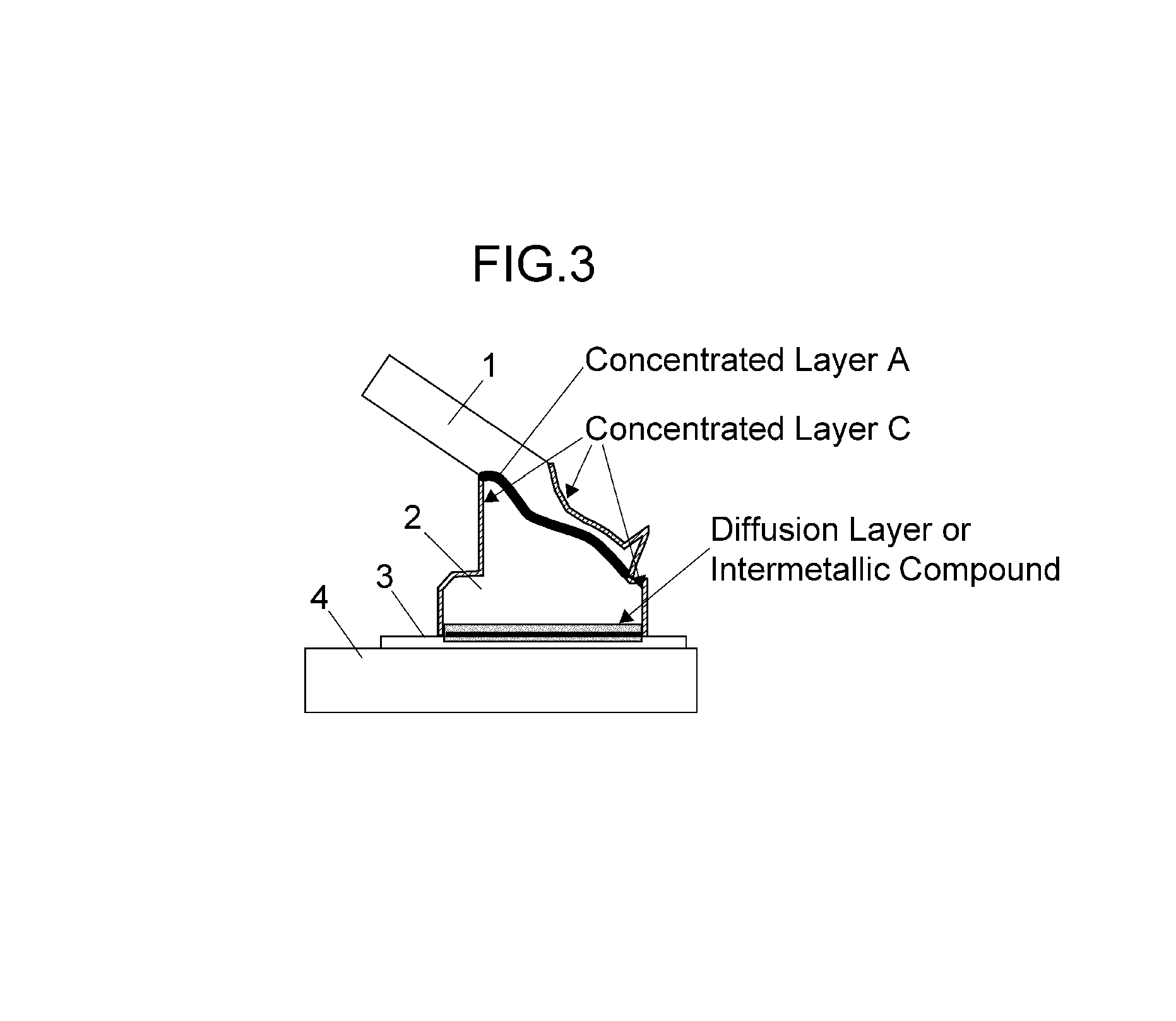
The invention is aimed at providing a bonding structure of a copper-based bonding wire, realizing low material cost, high productivity in a continuous bonding in reverse bonding for wedge bonding on bumps, as well as excellent reliability in high-temperature heating, thermal cycle test, reflow test, HAST test or the like. The bonding structure is for connecting the bonding wire onto a ball bump formed on an electrode of a semiconductor device, the bonding wire and the ball bump respectively containing copper as a major component thereof. The bonding structure comprises a concentrated layer A provided at an interface of a bonding part of the ball bump and the bonding wire, wherein the concentration of a metal R other than copper in the concentrated layer A is not less than ten times the average concentration of the metal R in the ball bump; and a concentrated layer B provided at an interface of a bonding part of the ball bump and the electrode, wherein the concentration of the metal R in the concentrated layer B is not less than ten times the average concentration of the metal R in the ball bump.

Description

CROSS REFERENCE TO PRIOR APPLICATIONS[0001]This application is a U.S. National Phase application under 35U.S.C. § 371of International Application No. PCT / JP2009 / 062635, filed on Jul. 10, 2009and claims benefit of priority to Japanese Patent Application No. 2008-181813, filed on Jul 11, 2008. The International Application was published in Japanese on Jan. 14, 2010as WO 2010 / 005086under PCT Article 21(2). All these applications are herein incorporated by reference.TECHNICAL FIELD[0002]The present invention relates to a bonding structure of a bonding wire used to connect electrodes on a semiconductor device by wiring them with circuit wiring substrates such as lead frames, substrates and tapes.BACKGROUND ART[0003]At present, a thin wire (bonding wire) having a wire diameter of about 20 to 50 μm is used mainly as the bonding wire bonding electrodes on a semiconductor device with external terminals. In order to bond the bonding wire, the ultrasonic wave-combined thermocompression bonding...

Claims


Application Information

Patent Timeline
Patent Type & Authority Patents(United States)
IPC IPC(8): H01L23/48H01L23/00
CPCH01L24/05H01L24/43H01L24/45H01L24/48H01L24/85H01L2924/20753H01L2924/20754H01L2924/20755H01L2924/20756H01L2924/20757H01L2924/3025H01L2224/45147H01L2924/01057H01L2924/0104H01L2924/01015H01L2924/01083H01L2924/01005H01L2224/48091H01L2924/00014H01L2924/01006H01L2924/00011H01L2924/01077H01L2224/05556H01L2224/05624H01L2924/01029H01L2924/01014H01L2224/45565H01L2224/45664H01L2224/45644H01L2224/45639H01L2224/45669H01L2224/45015H01L2924/20752H01L2924/20751H01L2224/04042H01L2224/05664H01L2224/4312H01L2224/4321H01L2224/4382H01L2224/43825H01L2224/43826H01L2224/43827H01L2224/45144H01L2224/4554H01L2224/45673H01L2224/45676H01L2224/4847H01L2224/48475H01L2224/85051H01L2224/85205H01L2924/01004H01L2924/01007H01L2924/01013H01L2924/01018H01L2924/01022H01L2924/01027H01L2924/01028H01L2924/01046H01L2924/01047H01L2924/01078H01L2924/01079H01L2924/01082H01L2924/01105H01L2924/01204H01L2924/01205H01L2924/01206H01L2924/01327H01L2924/10253H01L2924/14H01L2224/48486H01L2224/48499H01L2224/48011H01L2224/05639H01L2224/05644H01L2224/05647H01L2224/43848H01L2224/45572H01L2224/48471H01L2224/48507H01L2224/48511H01L2224/78301H01L2224/85045H01L2224/85065H01L2224/85075H01L2224/85186H01L2224/85207H01L2224/85439H01L2224/85444H01L2224/85986H01L2924/01024H01L2924/01033H01L2924/01044H01L2924/01045H01L2924/15311H01L2225/06562H01L2924/20105H01L2924/20106H01L2924/20107H01L2924/20108H01L2924/00015H01L2924/01001H01L2924/01203H01L2924/20758H01L2924/20759H01L2924/2076H01L2924/20109H01L2924/2011H01L2924/20111H01L2924/20652H01L2924/20655H01L2924/20645H01L2224/45124H01L2924/00H01L2224/48639H01L2224/48644H01L2224/48624H01L2224/48647H01L2224/48664H01L2224/48839H01L2224/48844H01L2224/48847H01L2224/48864H01L2224/48824H01L2224/48699H01L2924/013H01L2924/351H01L2224/48724H01L2224/48739H01L2224/48744H01L2224/48764H01L2224/48747Y10T428/12222H01L2224/85203H01L2224/45655H01L2224/45657H01L2224/45666H01L2224/45671H01L2924/01049
Inventor UNO, TOMOHIROYAMADA, TAKASHIIKEDA, ATSUO
Owner NIPPON MICROMETAL CO LTD
Learn More