
Sputtering target

a sputtering target and target technology, applied in the field of nb sputtering target, can solve the problems of deterioration of yield, difficult suppression of resistivity to 4 cm or less, and sudden eruption of giant dust such as exceeding 1 m, so as to reduce the ratio of grain size of adjacent grains, reduce the effect of stress difference generated in the course of grains recovering the strain and increase the yield of nb films

Inactive Publication Date: 2016-09-06
KK TOSHIBA
View PDF22 Cites 1 Cited by
  • Summary
  • Abstract
  • Description
  • Claims
  • Application Information

AI Technical Summary

Benefits of technology

The patent text discusses a method to improve the yield of Nb films or interconnection films. It explains that by reducing the ratio of grain sizes of the adjacent grains, stress difference can be alleviated and the occurrence of giant dust can be suppressed, resulting in a significant increase in yield. Additionally, the text mentions that oxides and intermetallic compounds formed during the process can increase the resistivity, which can be mitigated by using a certain target material. Overall, the patent presents a technical solution to enhance the quality and yield of films produced using sputtering technology.

Problems solved by technology

However, in semiconductor devices where further higher integration and densification are achieved, an existing stacking structure causes a poor coverage of an insulating film formed on the interconnection, resulting naturally in a deterioration of yield.
However, when with a Nb film deposited by use of an existing Nb target as the liner material, thereon an Al film or Al alloy film is deposited to form an Al interconnection film, it is difficult to suppress the resistivity to 4 μΩcm or less with reproducibility.
In addition, though being necessary to suppress admixture of dust in the interconnection film as much as possible, in the existing Nb target, there is a problem that giant dust such as exceeding 1 μm for instance occurs suddenly.
As a result, product yield of the semiconductor devices remarkably deteriorates.
Further, during deposition of the Nb liner film, the giant dust suddenly occurs to result in a decrease of the product yield of the semiconductor devices.
Thus, the existing Nb target faces a difficulty in applying in the next generation semiconductor memories or the like.

Method used


Image

  • Sputtering target
  • Sputtering target

Examples


embodiment 1

[0062]First, Nb2O5 containing concentrate of which Ta content is 3000 ppm or less is chemically processed to be a high purity oxide, the oxide being reduced by making use of thermite reduction method due to Al to obtain crude metal Nb.

[0063]Several pieces of such crude metal Nb are prepared. These are EB melted appropriately between one to multiple times to prepare 6 kinds of Nb ingots (diameter of 230 mm) different in the Ta content.

[0064]Each of these Nb ingots is drawn and forged to be a diameter of 130 mm, being annealed at a temperature of 1400° C., thereafter being forged again to be a diameter of 230 to 240 mm, and further being rolled by use of cross-rolling to be a disk of a diameter of 320 to 330 mm. To these disc-like Nb plates, heat treatment is applied under the conditions of 1100° C.×120 min to recrystallize.

[0065]The respective Nb plates after the aforementioned heat treatment are cut to be Nb plates for bonding, these and Al alloy plates for backing plate prepared in...

embodiment 2

[0070]Crude metal Nb prepared similarly with Embodiment 1 is EB melted three times to prepare an ingot. The Nb ingot undergoes plastic working under the conditions identical with Embodiment 1, thereafter by varying the heat treatment condition 6 kinds of Nb materials are prepared. The heat treatment temperatures are 300° C., 600° C., 800° C., 1100° C. and 1300° C., and treatment time periods are 60 min for all heat treatments. In addition, Nb material that is not heat-treated is prepared.

[0071]With such 6 kinds of Nb materials, similarly with Embodiment 1 Nb sputtering targets are prepared, respectively. The Ta content is analyzed due to an IPC-AES similarly with Embodiment 1. The Ta content is 1830 ppm, the dispersion thereof being 20%.

[0072]Next, with each of the aforementioned 6 kinds Nb sputtering targets, under the conditions of sputtering method of liner sputtering, a back pressure of 1×10⁻⁵ (Pa), a DC output of 15 (kW) and a sputtering time period of 1 (min), on a Si wafer (8...

embodiment 3

[0075]First, crude metals of Nb are prepared by varying oxygen contents. These are EB melted appropriately between one to multiple times to prepare 6 kinds of Nb ingots (diameter of 230 mm) of different oxygen contents.

[0076]Each of these Nb ingots is drawn and forged to be a diameter of 130 mm, being annealed at a temperature of 1400° C., thereafter being forged again to be a diameter of 230 to 240 mm, and further being rolled by use of cross-rolling to be a disk of a diameter of 320 to 330 mm. To these disc-like Nb plates, heat treatment is applied under the conditions of 1100° C.×120 min to recrystallize.

[0077]The respective Nb plates after the aforementioned heat treatment are cut to be Nb plates for bonding, these and Al alloy plates for backing plate prepared in advance being hot pressed under the conditions of a temperature of 400 to 600° C. and a pressure of 250 kg / cm2 to be bonded bodies that are target raw material. Each of thus obtained bonded bodies is machined to be a d...


PUM

PropertyMeasurementUnit
average grain diameteraaaaaaaaaa
temperatureaaaaaaaaaa
grain diameteraaaaaaaaaa

Abstract

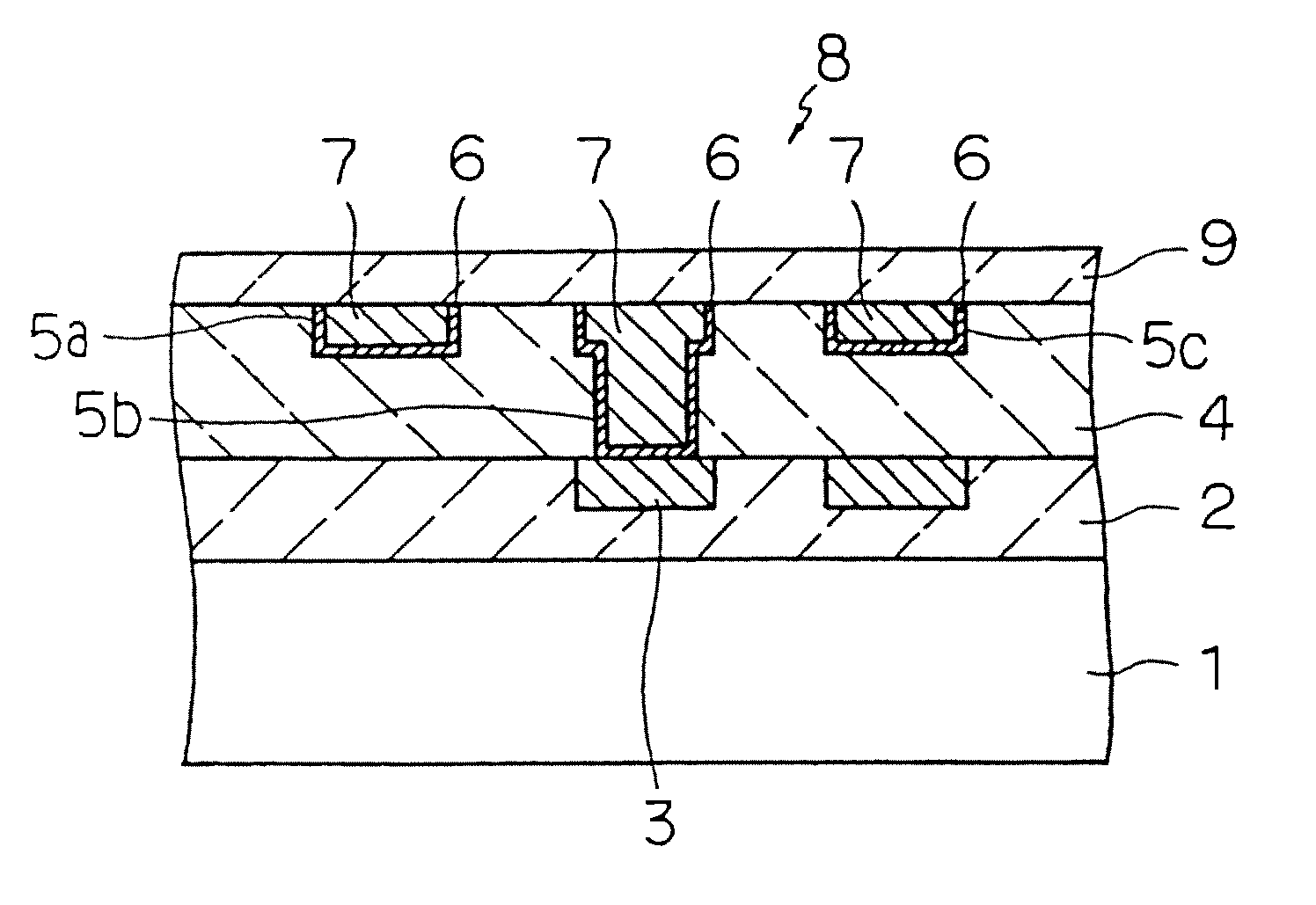
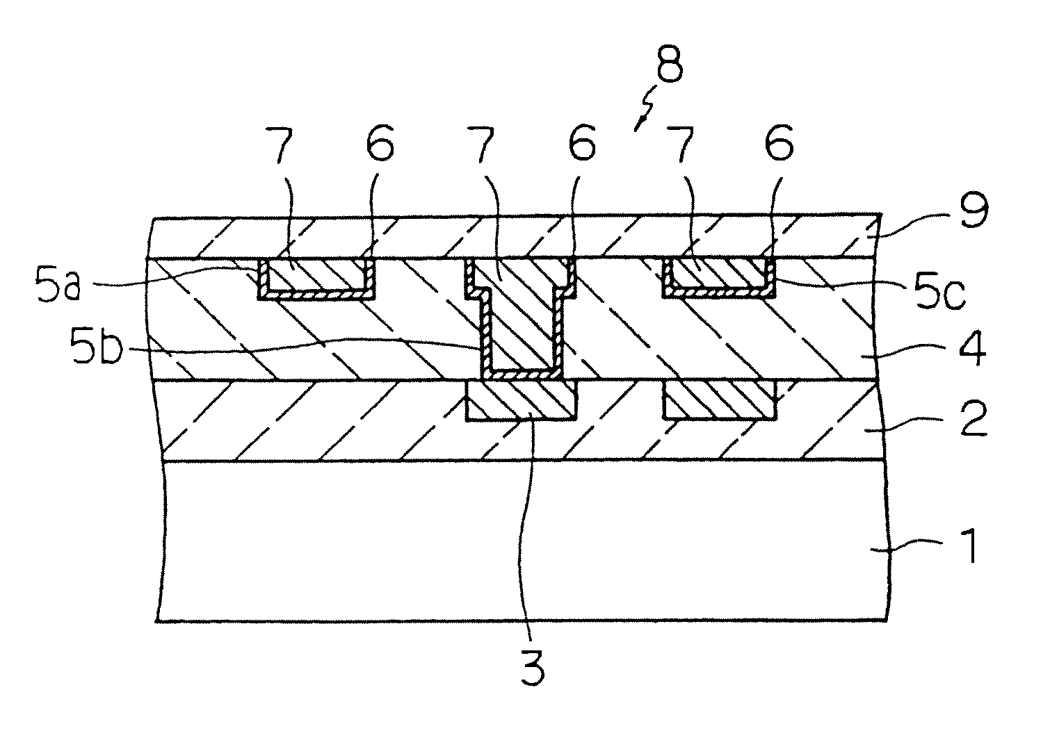
A sputtering target contains high purity Nb of which Ta content is 3000 ppm or less and oxygen content is 200 ppm or less. Dispersion of the Ta content in all the sputtering target is within ±30% as a whole target. Dispersion of the oxygen content is within ±80% as a whole target. According to such sputtering target, an interconnection film of low resistivity can be realized. In addition, each grain of Nb in the sputtering target has a grain diameter in the range of 0.1 to 10 times an average grain diameter and ratios of grain sizes of adjacent grains are in the range of 0.1 to 10. According to such sputtering target, giant dust can be largely suppressed from occurring. The sputtering target is suitable for forming a Nb film as liner material of an Al interconnection.

Description

CROSS-REFERENCE TO RELATED APPLICATIONS[0001]The present application is a Continuation of U.S. application Ser. No. 09 / 720,730, filed Dec. 29, 2000, now abandoned which is based upon PCT National Stage Application No. PCT / JP99 / 03407 filed Jun. 25, 1999, and claims the benefit of priority from prior Japanese Patent Application Nos. 10-182689, filed Jun. 29, 1998, 10-204001, filed Jul. 17, 1998 and 10-212829, filed Jul. 28, 1998, the entire contents of each of these applications are incorporated herein by reference.TECHNICAL FIELD[0002]The present invention relates to a Nb sputtering target suitable for forming liner material of a semiconductor element or the like.BACKGROUND ART[0003]In recent years, semiconductor industry typical in LSIs is increasing rapidly. In semiconductor elements of 64 Mbit DRAMs and subsequent ones, the higher the integration, reliability and functionality become, the higher accuracy is demanded for microfabrication technology. With such higher densification o...

Claims


Application Information

Patent Timeline
Patent Type & Authority Patents(United States)
IPC IPC(8): C22C27/02C23C14/34H01L21/285H01L21/768
CPCH01L21/76843C23C14/3414
Inventor WATANABE, KOICHIKOHSAKA, YASUOWATANABE, TAKASHIISHIGAMI, TAKASHISUZUKI, YUKINOBUFUJIOKA, NAOMI
Owner KK TOSHIBA
Learn More