Integrated circuit (IC) design method with enhanced circuit extraction models

a technology of integrated circuits and extraction models, applied in the field of integrated circuit design technologies, can solve the problems of limiting the design margin, thinning and densifying the interconnect, and limiting the performance of nano-scale integrated circuits

Active Publication Date: 2016-10-18
SHANGHAI INTEGRATED CIRCUIT RES & DEV CENT
View PDF3 Cites 0 Cited by
  • Summary
  • Abstract
  • Description
  • Claims
  • Application Information

AI Technical Summary

Benefits of technology

[0060]By using the disclosed methods and systems, novel techniques can be developed to perform correlation-considered statistical interconnect parasitic parameters extraction based on, for example, a 40 nm CMOS process technology. Interconnect Technology Profile (ITP) file can be carefully calibrated using 3D simulations based on a comprehensive set of test structures and full mapping tests are performed on these structures to obtain statistical distribution of the layout parasitics. With the statistical data and process information, statistical ITP parameters are extracted using Principal Component Analysis (PCA) method and verified with circuit level verification. The extracted statistical ITP may be accurate and necessary for neon-scale IC process technologies. The issues of the conventional techniques, such as etching damages to the metal film resistor when forming upper copper interconnect to connect the metal film resistor, can be solved and the reliability of the metal film resistor can be substantially increased. Those of ordinary skill in the art can make changes and modifications without departing from the principles and spirits of the present invention.

Problems solved by technology

However, as the IC process technology scales into sub-100 nm, the interconnects become thinner and denser.
The performance of nano-scale integrated circuits may be limited because RC delay becomes no less than MOSFET gate delay.
Although this method allows IC designers to sign off a design with extreme process conditions, it limits the design margin and may cause overhead in the design.

Method used


Image

  • Integrated circuit (IC) design method with enhanced circuit extraction models
  • Integrated circuit (IC) design method with enhanced circuit extraction models
  • Integrated circuit (IC) design method with enhanced circuit extraction models

Examples


Embodiment Construction

[0017]Reference will now be made in detail to exemplary embodiments of the invention, which are illustrated in the accompanying drawings. Wherever possible, the same reference numbers may be used throughout the drawings to refer to the same or like parts.

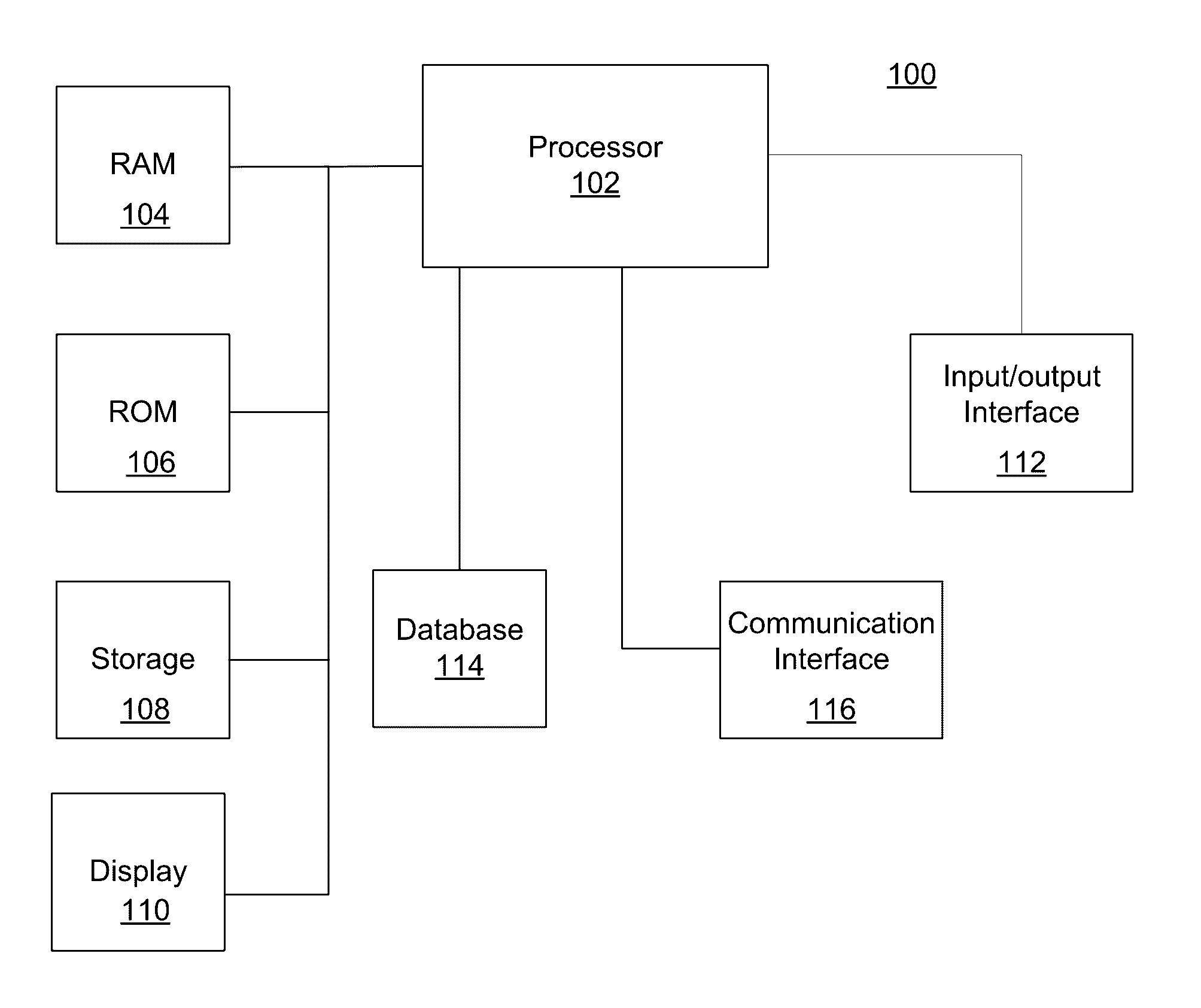
[0018]FIG. 1 shows an exemplary block diagram of an electronic design automation (EDA) system 100. The EDA system 100 may include any appropriately configured computer system. As shown in FIG. 1, system 100 may include a processor 102, a random access memory (RAM) unit 104, a read-only memory (ROM) unit 106, a storage unit 108, a display 110, an input / output interface unit 112, a database 114; and a communication interface 116. Other components may be added and certain devices may be removed without departing from the principles of the disclosed embodiments.

[0019]Processor 102 may include any appropriate type of general purpose microprocessor, digital signal processor or microcontroller, and application specific integrated circuit (...


PUM


Abstract

A method is provided for designing an IC chip. The method includes receiving data from a pre-layout design process for the IC chip, routing a plurality of interconnecting wires to connect various devices of the IC chip, and extracting various circuit parameters. The method also includes simulating the IC chip using the extracted various circuit parameters to detect logic or timing error in the IC chip. The extracting the various circuit parameters includes establishing a statistical interconnect technology profile (ITP) file containing at least interconnect parasitic parameters based on correlations of interconnect layer geometric parameter variations.

Description

CROSS-REFERENCES TO RELATED APPLICATIONS[0001]This application claims the priority of Chinese patent application number 201210249620.X, filed on Jul. 18, 2012, the entire contents of which are incorporated herein by reference.FIELD OF THE INVENTION[0002]The present invention generally relates to the field of integrated circuit (IC) design technologies and, more particularly, to techniques improving post-layout design during the IC design and fabrication process.BACKGROUND[0003]Electronic design automation (EDA) software for integrated circuit (IC) has rapidly increased in importance with the continuous scaling of semiconductor technology. An IC design software often needs various simulation steps to optimize the circuit design parameters, such as pre-layout simulation and post-layout simulation, etc. However, as the IC process technology scales into sub-100 nm, the interconnects become thinner and denser. The performance of nano-scale integrated circuits may be limited because RC de...

Claims


Application Information

Patent Timeline
Patent Type & Authority Patents(United States)
IPC IPC(8): G06F17/50
CPCG06F17/5077G06F17/5009G06F17/5068G06F17/5081G06F30/39G06F30/394G06F30/20G06F30/398
Inventor REN, ZHENGHU, SHAOJIANZHOU, WEICHEN, SHOUMIANZHAO, YUHANG
Owner SHANGHAI INTEGRATED CIRCUIT RES & DEV CENT
Why Eureka
Try Eureka