

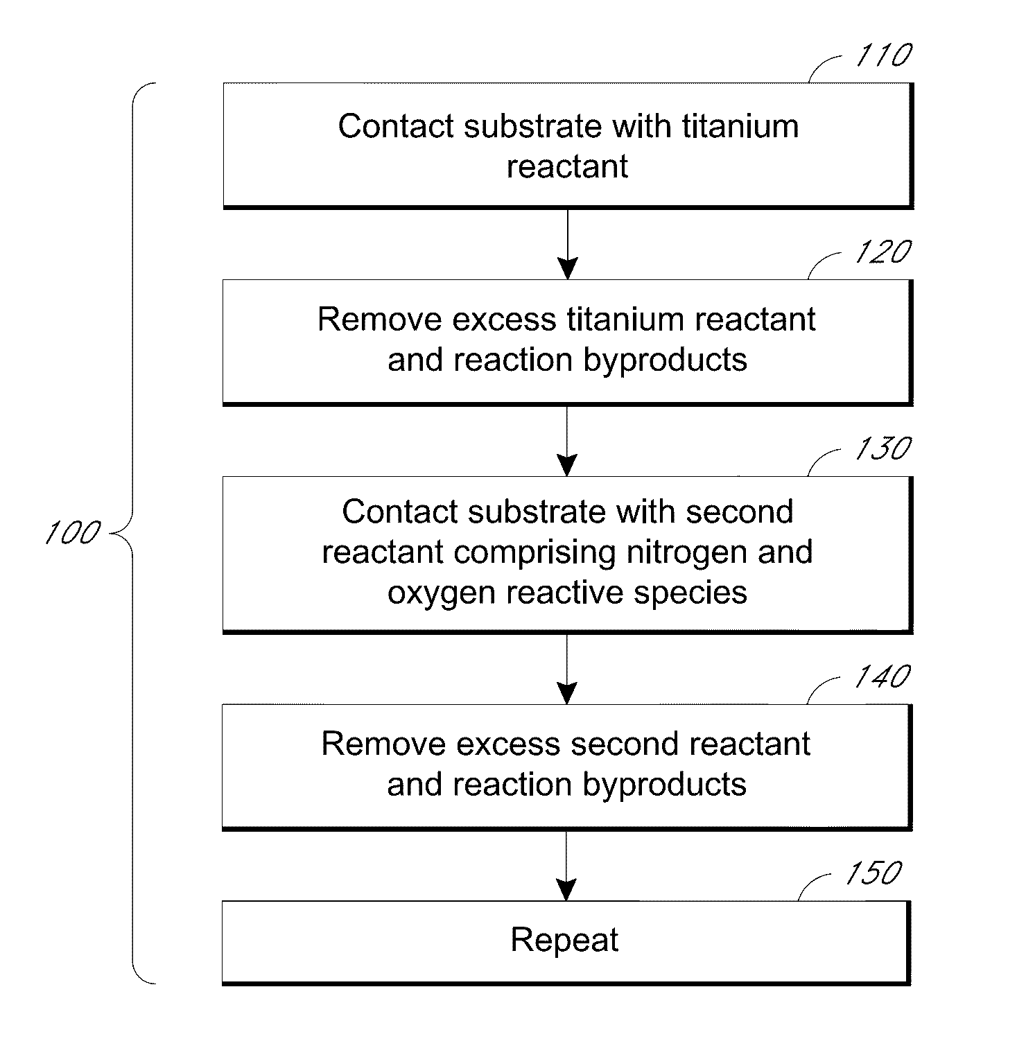
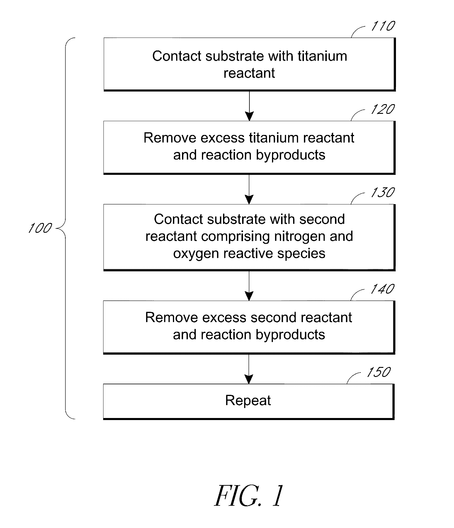
Process for deposition of titanium oxynitride for use in integrated circuit fabrication
a technology of titanium oxynitride and integrated circuit, which is applied in the direction of chemical vapor deposition coating, solid-state devices, coatings, etc., can solve the problems of inability to reliably form photolithographic techniques, inability to meet the requirements of the intended use of spacers, and the minimum pitch of photolithographic techniques is an obstacle to the reduction of feature siz
- Summary
- Abstract
- Description
- Claims
- Application Information
AI Technical Summary
Benefits of technology
Problems solved by technology
Method used
Image

Examples
example 1
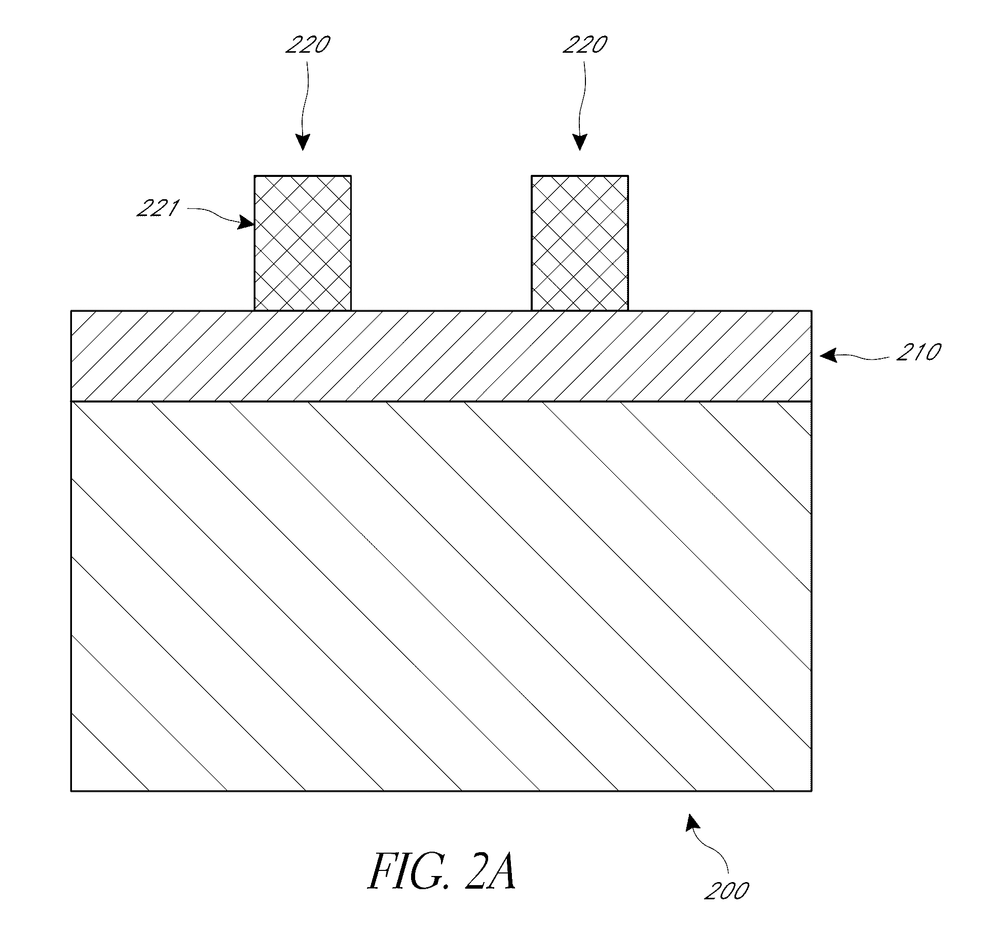
[0097]A TiOxNy thin film was deposited according to the present disclosure by a PEALD process using TDMAT as the titanium precursor and O2+N2 plasma as the second reactant. A susceptor temperature of 190° C. was used. Plasma power was about 400 W and the RF on time was about 0.2 seconds. The second reactant was flowed into the chamber with the aid of an Ar carrier gas. The carrier gas flow rate was about 2 slm. The O2 flow rate was about 0.1 slm while the N2 flow rate was about 1.9 slm.
[0098]In addition to the TiOxNy thin film that was deposited, a titanium oxide reference film was deposited. The titanium oxide thin film was deposited by a PEALD processing using TDMAT as the titanium precursor and O2 plasma as the second reactant. The titanium oxide thin film was deposited at the same susceptor temperature, plasma power, and pressure as the TiOxNy thin film. The second reactant was flowed into the chamber with the aid of an Ar carrier gas. The carrier gas flow rate was about 2 slm. ...
PUM
| Property | Measurement | Unit |
|---|---|---|
| temperature | aaaaa | aaaaa |
| temperature | aaaaa | aaaaa |
| RF power | aaaaa | aaaaa |
Abstract
Description
Claims
Application Information