

TFT substrate structure and manufacturing method thereof
a thin film transistor and substrate technology, applied in the field of display technology, can solve the problems of increased operation current (ion) of the tft substrate structure, difficult to form an ohmic contact, and large potential difference between a-si materials, so as to improve the reliability, increase the current efficiency, and improve the effect of current efficiency
- Summary
- Abstract
- Description
- Claims
- Application Information
AI Technical Summary
Benefits of technology
Problems solved by technology
Method used
Image

Examples
first embodiment
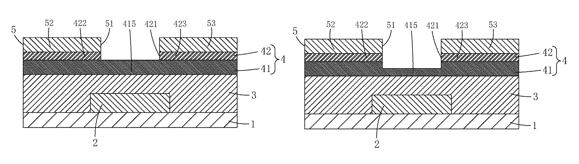
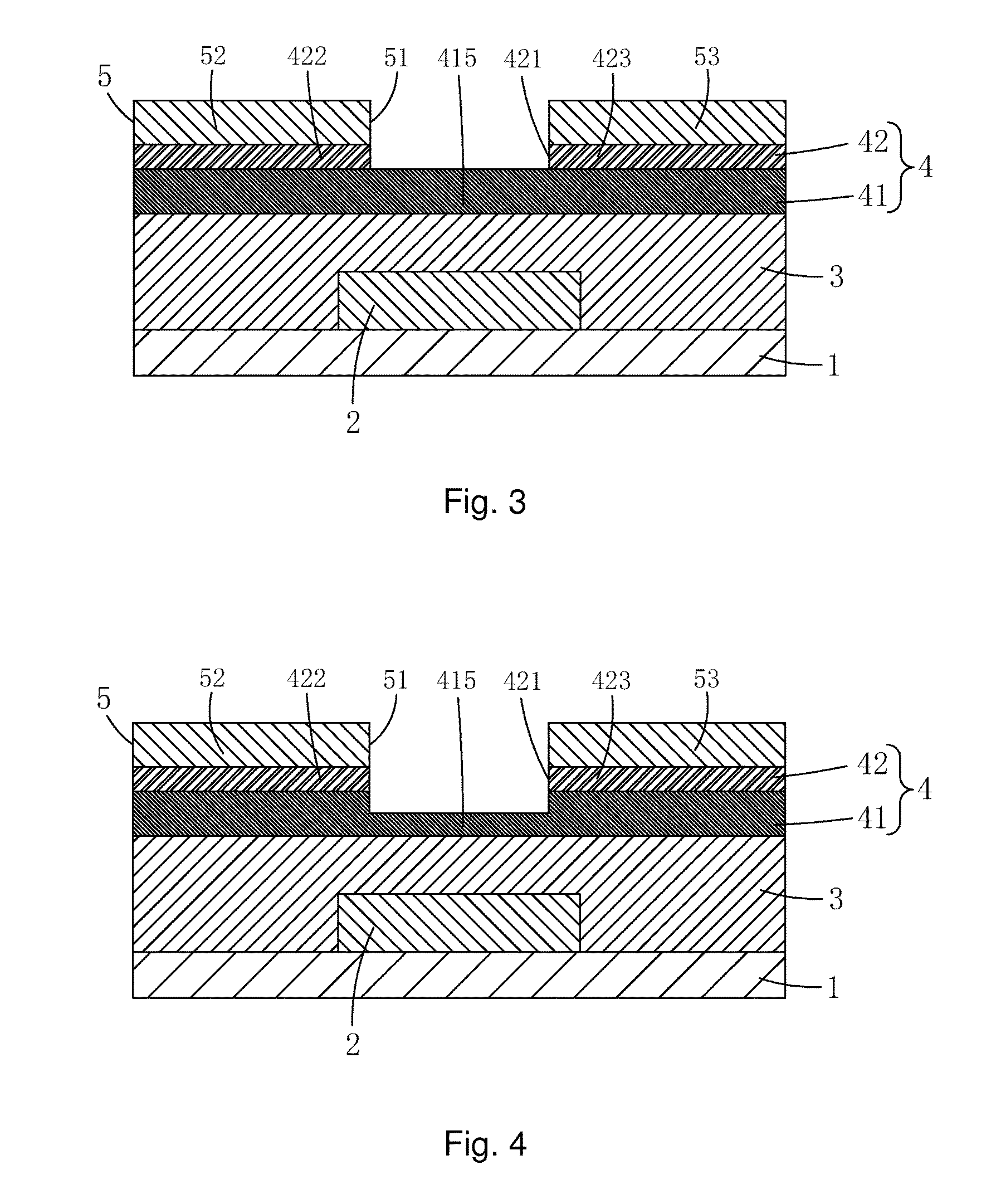
[0052]As shown in FIG. 3, a schematic view, in a sectioned form, is provided to illustrate the TFT substrate structure according to the present invention, in which the portion of the amorphous silicon layer 41 that is located in the channel zone 415 has a thickness that is equal to a thickness of a remaining portion thereof.
second embodiment
[0053]As shown in FIG. 4, a schematic view, in a sectioned form, is provided to illustrate the TFT substrate structure according to the present invention, in which the portion of the amorphous silicon layer 41 that is located in the channel zone 415 has a thickness that is less than a thickness of a remaining portion thereof.
[0054]Specifically, the base plate 1 comprises a glass board.
[0055]The gate terminal 2, the source terminal 52, and the drain terminal 53 each comprise a material of one of molybdenum, titanium, aluminum, and copper or a stacked combination of multiple ones thereof.
[0056]The gate insulation layer 3 comprises a material of silicon oxide, silicon nitride, or a combination thereof.
[0057]Specifically, the metal oxide semiconductor layer 5 comprises a material of IGZO (Indium Gallium Zinc Oxide).
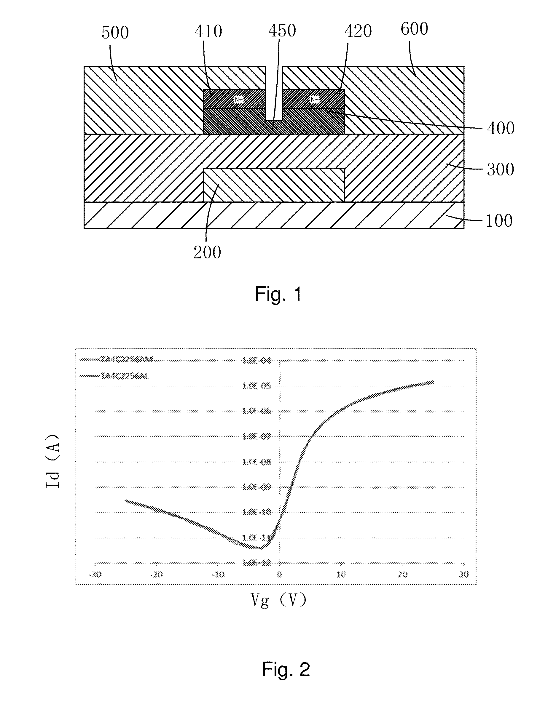
[0058]FIG. 5 shows a comparison between a curve of a leakage current of an amorphous silicon (a-Si) device involving a TFT substrate structure illustrated in FIG. 1 and a cur...
PUM
| Property | Measurement | Unit |
|---|---|---|
| thickness | aaaaa | aaaaa |
| surface area | aaaaa | aaaaa |
| semiconductor | aaaaa | aaaaa |
Abstract
Description
Claims
Application Information