
Metal-dielectric hybrid surfaces as integrated optoelectronic interfaces

a technology of dielectric hybrid surfaces and optoelectronic interfaces, applied in the direction of transmission, semiconductor devices, photovoltaic energy generation, etc., can solve the problem of unrivaled performan

Active Publication Date: 2017-01-03
THE BOARD OF TRUSTEES OF THE LELAND STANFORD JUNIOR UNIV
View PDF6 Cites 1 Cited by
  • Summary
  • Abstract
  • Description
  • Claims
  • Application Information

AI Technical Summary

Benefits of technology

[0006]In one aspect, the present invention provides a new optoelectronic device in which the two important elements of conventional designs, photon management structures and transparent conductors, are united in a single structure that offers performance not possible in traditional designs: an effective optoelectronic interface comprising dielectric nano-element arrays protruding through a conductive metal film, thereby providing a surface with high metal coverage, and thus high conductivity, while allowing coupling of light and absorption into an underlying substrate.
[0007]This surprising design represents a fundamentally new paradigm for designing hybrid optoelectronic surfaces where transparent electrodes and photon management nanostructures are integrated into a single interface for maximum performance.
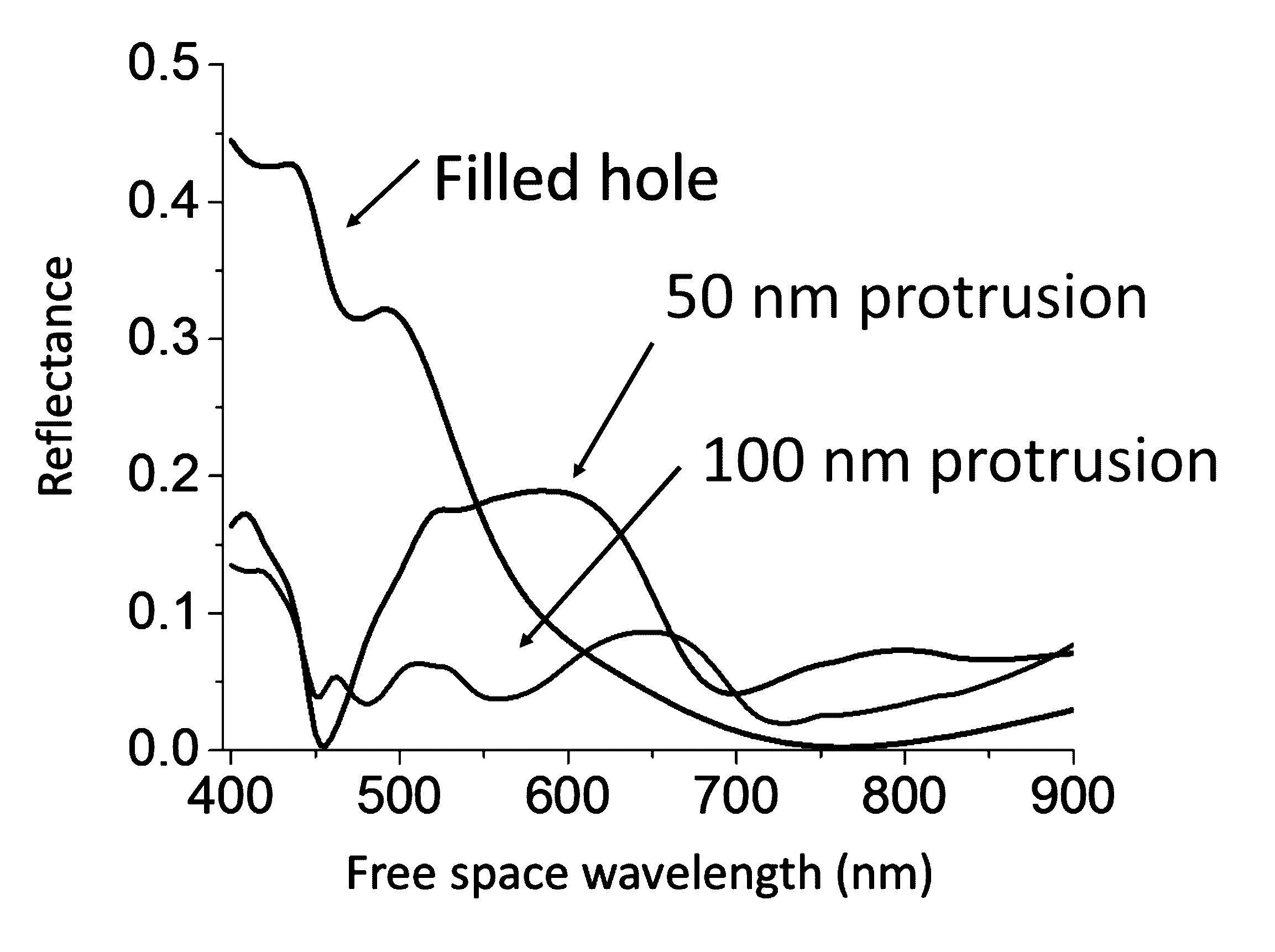
[0008]The design lifts the restriction for low metal coverage, allowing structures that have significantly lower sheet resistance values than technology currently available. In one aspect, the structure comprises an array of dielectric resonant elements with an embedded metal film. The metal film is disposed below the top surface of the resonant elements. Owing to leaky resonances within the resonant elements, light is concentrated in each resonator and can couple between the outside world and the substrate through the small volume beneath each resonant element; the metal film is thus virtually invisible to light, allowing designs with extremely high absorption (>90%) and low sheet resistance (<20 Ohm / sq.) despite having extremely high (50% or greater) metal coverage. Electromagnetic simulations show that across a wide range of materials and geometries, leaky Mie resonances in the nanopillars direct electromagnetic energy around the metal film and into the underlying substrate. The hybrid metal-dielectric surface is a unique structure that offers unparalleled performance in applications when a transparent conductor in contact with a high-refractive index medium is needed.
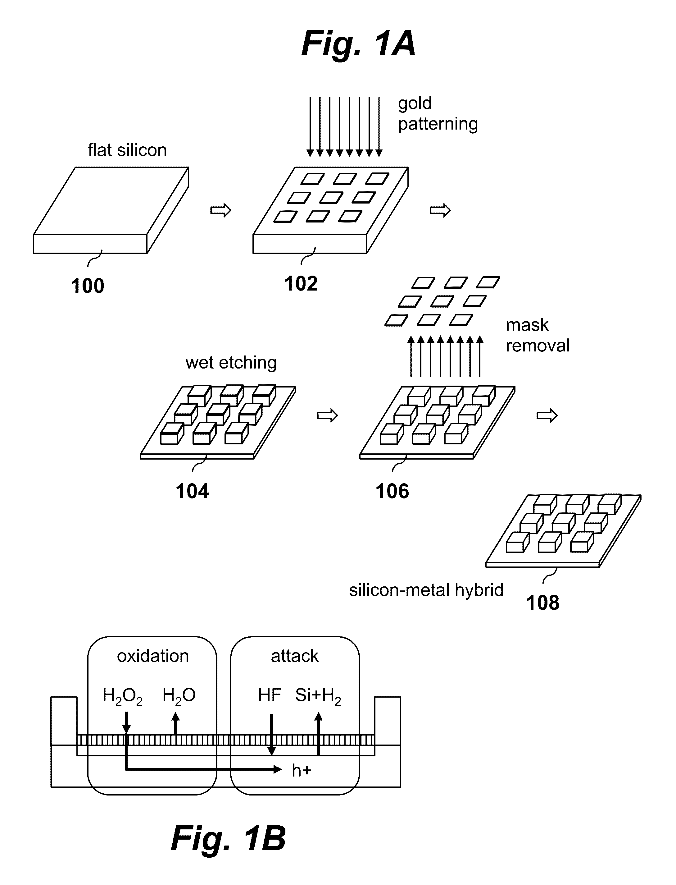
[0019]Further, in some embodiments, the structure is fabricated using metal-assisted chemical etching (MACE). In MACE, a patterned metal in direct contact with a dielectric surface acts as a catalyst for wet etching: the metal sinks into the dielectric as the reaction proceeds and is thus automatically self-aligned to the nanostructure it creates. The MACE process is simple and versatile, and compatible with a number of combinations of metals and optically important semiconductors, including silicon, gallium arsenide, and indium phosphide.

Problems solved by technology

The hybrid metal-dielectric surface is a unique structure that offers unparalleled performance in applications when a transparent conductor in contact with a high-refractive index medium is needed.

Method used


Image

  • Metal-dielectric hybrid surfaces as integrated optoelectronic interfaces
  • Metal-dielectric hybrid surfaces as integrated optoelectronic interfaces
  • Metal-dielectric hybrid surfaces as integrated optoelectronic interfaces

Examples


Embodiment Construction

[0029]To maximize light coupling or absorption, optoelectronic devices typically contain light management structures of high index materials, either in an active or window layer. These could include micro- and nano-pillars, cones, wires, pyramids and inverted pyramids, spheres, shells, domes, and other geometries. These light management structures improve light coupling through gradual refractive index matching, scattering, coupling to guided modes, and photonic crystal effects.

[0030]These light management structures typically sit in close proximity to electrodes in the device which allow for electrical contact. Electrodes can be made of transparent conductors, notably oxides, which offer some conductivity while permitting light transmission through a continuous film of material. Sputtered indium-doped tin oxide (ITO) is the most common transparent conductor currently used; however, sputtering ITO evenly over highly textured surfaces can be challenging, and the thick layers needed f...


PUM

PropertyMeasurementUnit
wavelength bandwidthaaaaaaaaaa
thicknessaaaaaaaaaa
wavelengthsaaaaaaaaaa

Abstract

An optoelectronic device has a hybrid metal-dielectric optoelectronic interface including an array of nanoscale dielectric resonant elements (e.g., nanopillars), and a metal film disposed between the dielectric resonant elements and below a top surface of the resonant elements such that the dielectric resonant elements protrude through the metal film. The device may also include an anti-reflection coating. The device may further include a metal film layer on each of the dielectric resonant elements.

Description

CROSS-REFERENCE TO RELATED APPLICATIONS[0001]This application claims priority from U.S. Provisional Patent Application 62 / 155,396 filed Apr. 30, 2015, which is incorporated herein by reference.STATEMENT OF GOVERNMENT SPONSORED SUPPORT[0002]This invention was made with Government support under contract DE-EE0004946 awarded by the Department of Energy. The Government has certain rights in the invention.FIELD OF THE INVENTION[0003]The present invention relates generally to optoelectronic devices such as photovoltaic devices, photosensors, and light-emitting diodes (LEDs). More specifically, it relates to an improved optoelectronic interface for such devices.BACKGROUND OF THE INVENTION[0004]A variety of nanostructured surfaces, including nanopillars, nanocones, nanowires, inverted pyramids, nanospheres, nanoshells, and nanodomes, have enabled strong, broadband absorption in semiconductors for optoelectronic devices such as photosensors and photovoltaics. Dielectric nanostructures are ex...

Claims


Application Information

Patent Timeline
Patent Type & Authority Patents(United States)
IPC IPC(8): H04B5/00H01L31/0224H01L31/0216H01L31/0687H01L31/0725H01L31/0236H01L33/38H01L31/0232H01L33/44
CPCH01L31/02327H01L31/0224H01L31/02161H01L31/02168H01L31/02366H01L31/022425H01L31/0687H01L31/0725H01L33/38H01L33/44H01L2933/0016H01L31/0232H01L33/405H01L33/60Y02E10/544Y02E10/50
Inventor NARASIMHAN, VIJAY K.HYMEL, THOMAS M.LAI, RUBY A.CUI, YI
Owner THE BOARD OF TRUSTEES OF THE LELAND STANFORD JUNIOR UNIV
Learn More