

Semiconductive roller and production method therefor
a semi-conductive roller and production method technology, applied in the field of semi-conductive rollers, can solve the problems of increasing the production cost reducing the productivity of the semi-conductive roller, and difficult to obtain and handle ion-conductive rubber and other problems, to achieve the effect of reducing costs, reducing production costs, and suppressing variations in electrical resistan
- Summary
- Abstract
- Description
- Claims
- Application Information
AI Technical Summary
Benefits of technology
Problems solved by technology
Method used
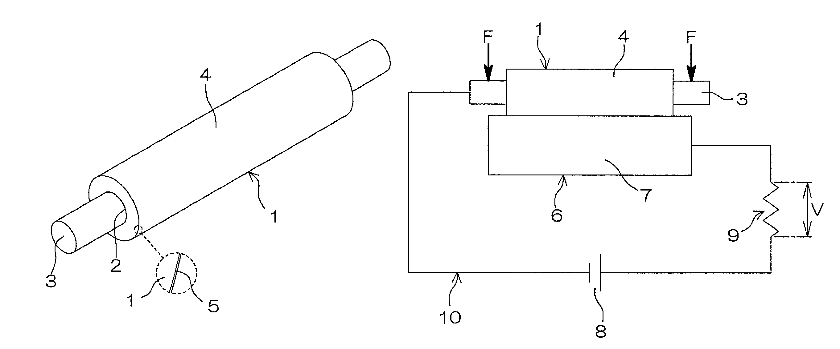
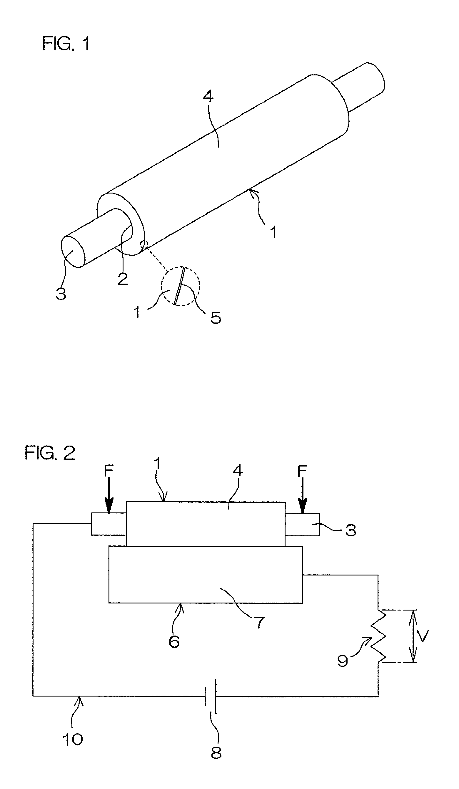
Image

Examples
example 1
[0105]First, 70 parts by mass of an NBR (lower-acrylonitrile content NBR JSR (registered trade name) N250SL of non-oil-extension type available from JSR Co., Ltd., and having an acrylonitrile content of 19.5%) and 30 parts by mass of an EPDM (ESPRENE (registered trade name) 505A of non-oil-extension type available from Sumitomo Chemical Co., Ltd., and having an ethylene content of 50% and a diene content of 9.5%) were simply kneaded as a rubber component by means of a 9-L kneader, and ingredients shown below in Table 1 were added to the rubber component in the aforementioned manner. The resulting mixture was further kneaded. Thus, a rubber composition was prepared.
[0106]The mass ratio between the NBR and the EPDM was NBR / EPDM=70 / 30.
[0107]
TABLE 1IngredientsParts by massISAF30Sulfur powder1.50Accelerating agent CZ1.00Peroxide crosslinking agent2.00Zinc oxide Type 25
[0108]The ingredients shown in Table 1 are as follows: ISAF: Carbon black (SEAST 6 available from Tokai Carbon Co., Ltd.)...
PUM
| Property | Measurement | Unit |
|---|---|---|
| roller resistance | aaaaa | aaaaa |
| roller resistance | aaaaa | aaaaa |
| thickness | aaaaa | aaaaa |
Abstract
Description
Claims
Application Information