Process for manufacturing a semiconductor device comprising an empty trench structure and semiconductor device manufactured thereby

a manufacturing process and semiconductor technology, applied in the manufacture of electrode systems, electric discharge tubes/lamps, tubes with electrostatic control, etc., can solve the problems of inability to ensure that the metal does not penetrate the trenches in large amounts, the metal layer is difficult to be deposition, and the device is not always properly operated

Active Publication Date: 2017-01-24
STMICROELECTRONICS SRL
View PDF8 Cites 2 Cited by
  • Summary
  • Abstract
  • Description
  • Claims
  • Application Information

AI Technical Summary

Benefits of technology

[0017]In one embodiment, in order to prevent penetration of metal material into the trench, during at least part of etching thereof, the products of reaction of a polymeric type, instead of being removed with the subsequent processes of resist removal, are left, as deposited, on the walls of the trench. In this way, on these, a passivation layer is formed, which, in the proximity of the open end or mouth of the trench, forms a sort of narrowing that restricts the area of the mouth itself. By modulating appropriately the etching conditions, said narrowing forms a “collar” element that prevents penetration of the metal material, for example aluminum, into the trench during the subsequent step of deposition of the cathode layer. In addition, the collar forms a sort of “mold”, which gives rise to a tip shape of the cathode region, which optimizes the performance of the finished device.

Problems solved by technology

In the practical manufacture of the device, there have been noted difficulties in deposition of the metal layer that is to form the cathode metal region 11.
In fact, even using non-conformable material and deposition techniques, it is not always possible to guarantee that the metal does not penetrate extensively within the trench 10.
Furthermore, the presence of metal particles inside the trench is disadvantageous given that any possible metal traces in the trench 10 may give rise to leakage that cannot be easily distinguished from emissions of the cathode metal region, resulting in an improper operation of the device.
This requirement, also in common with other empty trench semiconductor products, is not easy to meet, given the absence of a stop structure, also taking into account the conditions of negative pressure present in certain applications.

Method used


Image

  • Process for manufacturing a semiconductor device comprising an empty trench structure and semiconductor device manufactured thereby
  • Process for manufacturing a semiconductor device comprising an empty trench structure and semiconductor device manufactured thereby
  • Process for manufacturing a semiconductor device comprising an empty trench structure and semiconductor device manufactured thereby

Examples


Embodiment Construction

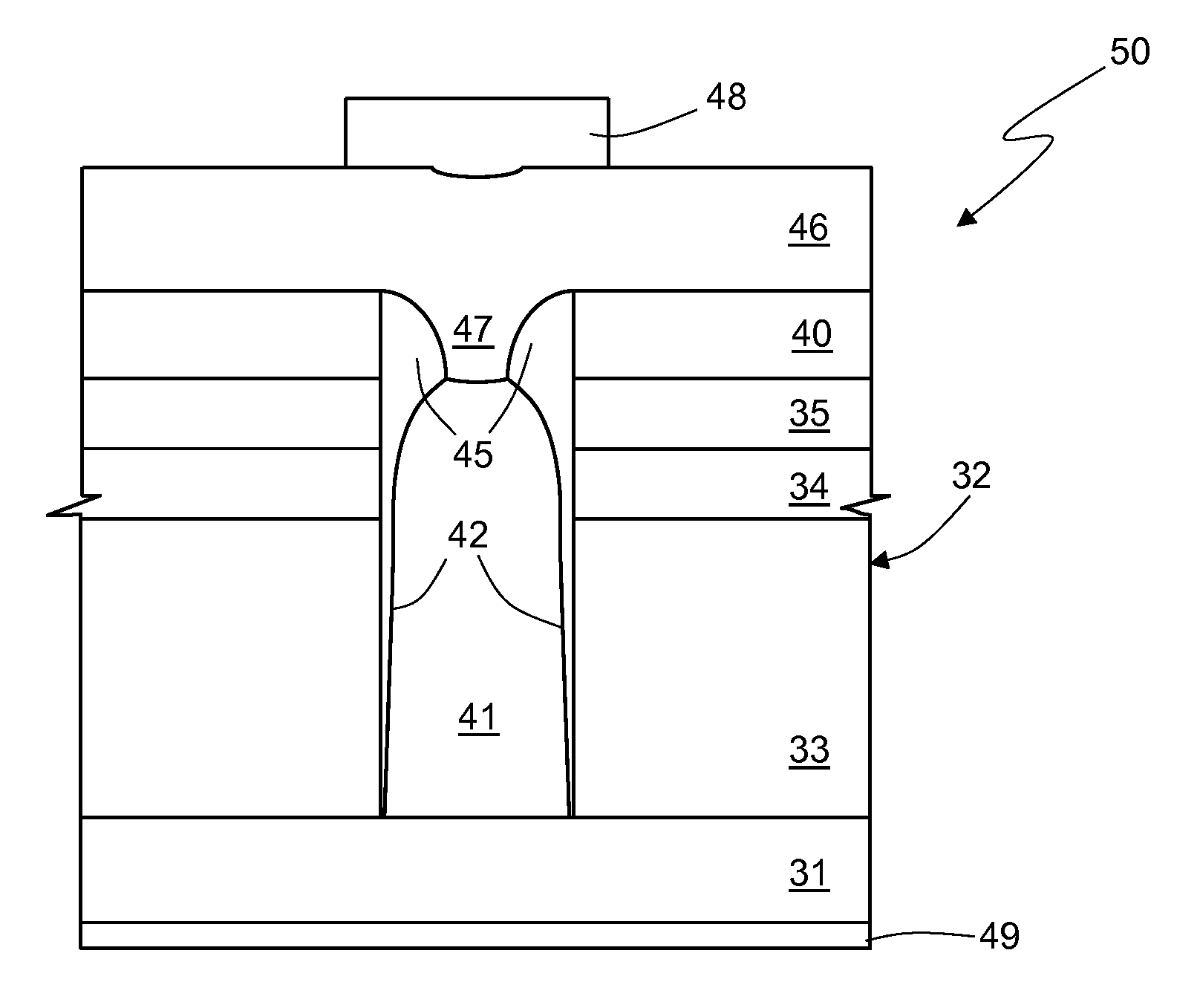
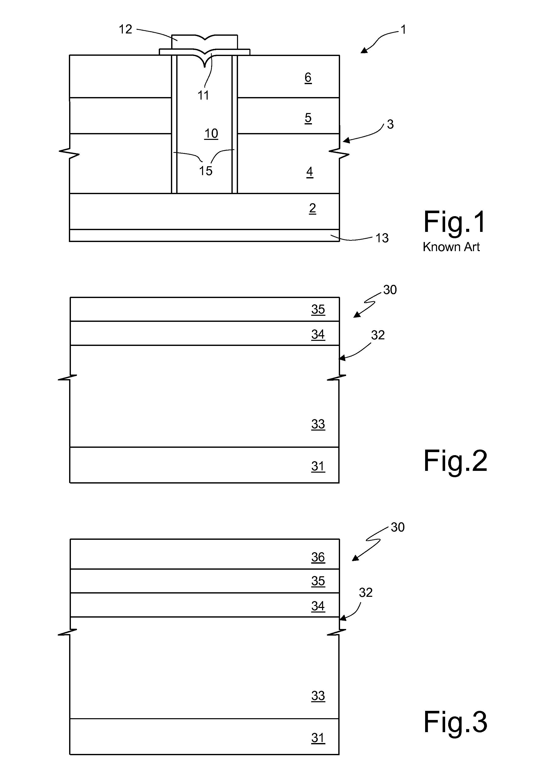
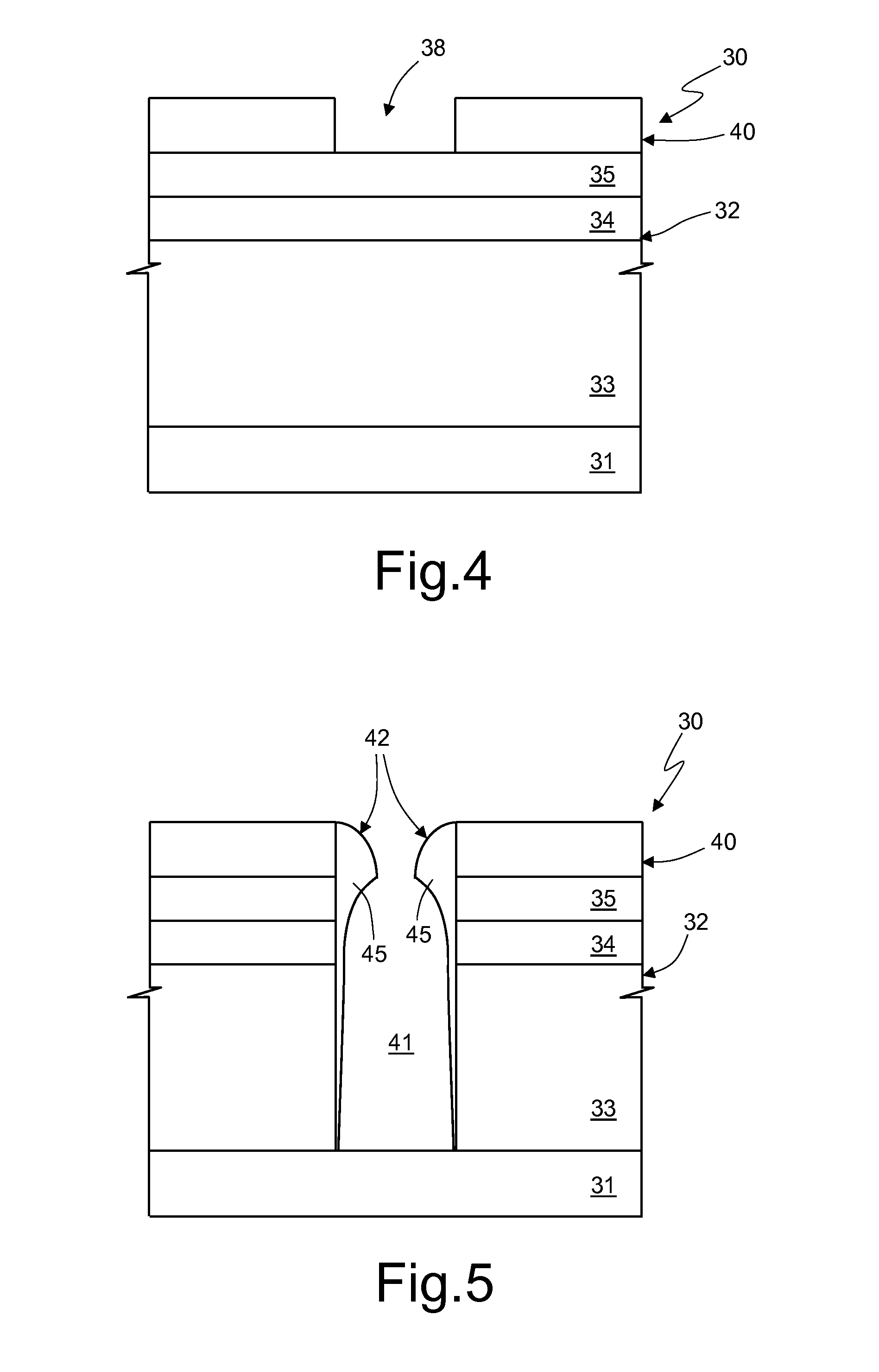
[0022]An embodiment of the present process for manufacturing the above device is described hereinafter, with reference to FIGS. 2-7.

[0023]In particular, the process described regards manufacture of an empty trench microelectronic semiconductor device, such as a diode, a triode, a tetrode, a pentode or some other device having a similar basic structure.

[0024]Initially (FIG. 2), on a substrate 31, of heavily doped semiconductor material, such as monocrystalline silicon, a stack 32 of layers is formed. The ensemble constituted by the substrate 31 and the stack 32 forms a body 30, for example a wafer.

[0025]The substrate 31 is typically of an N type, for example doped with phosphorus, and has a resistivity of approximately 4 mΩ·cm.

[0026]The stack 32 here comprises a first insulating layer 33, a conductive layer 34, and a second insulating layer 35.

[0027]For example, the first insulating layer 33 is made of tetraethylorthosilicate (TEOS) formed by chemical vapor deposition (CVD) with a th...


PUM


Abstract

The process is based upon the steps of: forming a trench in a body including a substrate and at least one insulating layer; and depositing a metal layer above the body for closing the open end or mouth of the trench. The trench is formed by selectively etching the body, wherein the reaction by-products deposit on the walls of the trench and form a passivation layer along the walls of the trench and a restriction element in proximity of the mouth of the trench.

Description

BACKGROUND[0001]Technical Field[0002]The present disclosure relates to a process for manufacturing a semiconductor device comprising an empty trench structure, and a semiconductor device obtained with said process.[0003]Description of the Related Art[0004]In the present context, the term “empty trench” refers to the fact that the trench (or some other cavity of any shape) is not filled, irrespective of the conditions of pressure existing inside the trench itself.[0005]In semiconductors devices it is at times required to provide an empty trench. For example, empty-channel transistor devices are under study (also called “microminiature vacuum tubes” or “vacuum microelectronic devices”—VMDs) present in which is a very deep trench closed at the top by a layer of metal, for example aluminum, which operates as ion-emitter element.[0006]An example of an embodiment of an empty trench microelectronic device and its manufacturing method are described, for example, in U.S. Patent Publication N...

Claims


Application Information

Patent Timeline
Patent Type & Authority Patents(United States)
IPC IPC(8): H01L21/00H01J21/10H01J9/02H01L29/861H01L29/06H01J19/24H01L29/66H01L21/308H01L21/3065H01J21/04
CPCH01L29/861H01J9/025H01J19/24H01J21/04H01J21/105H01L21/3065H01L21/3081H01L29/6609H01L29/4236
Inventor FIUMARA, ANTONINO
Owner STMICROELECTRONICS SRL
Why Eureka
Try Eureka