Semiconductor structure and method of forming the same

a technology of semiconductors and semiconductors, applied in the direction of semiconductor devices, semiconductor/solid-state device details, electrical apparatus, etc., can solve the problems of uneven voltage distribution through the channel, affecting the quality of fin-fet, and no longer meeting the requirements of current planar transistors, etc., to achieve easy formation and improve the yield of products

Active Publication Date: 2017-04-04
UNITED MICROELECTRONICS CORP
View PDF4 Cites 1 Cited by
  • Summary
  • Abstract
  • Description
  • Claims
  • Application Information

AI Technical Summary

Benefits of technology

[0007]For achieving a device with better electrical performance, the present invention therefore provides a semiconductor structure that is easy to fabricate.
[0010]Since the first patterned mask layer and the second patterned mask layer have patterns that are easy to form, the yields of the product can be upgraded. According to different embodiments, novel shapes of the contact plugs can also be provided.

Problems solved by technology

However, with the miniaturization development of the electronic products, current planar transistors no longer meet the requirements of the products.
However, due to the three-dimensional structure of the Fin-FET, a lot of drawbacks raises as well.
For example, in conventional Fin-FET, the fin structure includes a corner with a nearly 90 degrees, which may result in uneven voltage distribution through the channel.
Consequently, the quality of the Fin-FET is affected.

Method used


Image

  • Semiconductor structure and method of forming the same
  • Semiconductor structure and method of forming the same
  • Semiconductor structure and method of forming the same

Examples


Embodiment Construction

[0016]To provide a better understanding of the presented invention, preferred embodiments will be detailed. The preferred embodiments of the present invention are illustrated in the accompanying drawings with numbered elements.

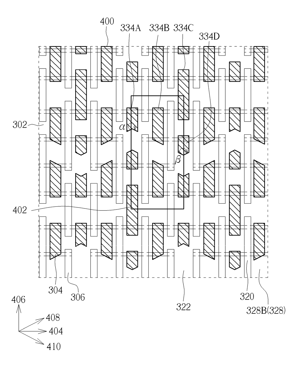
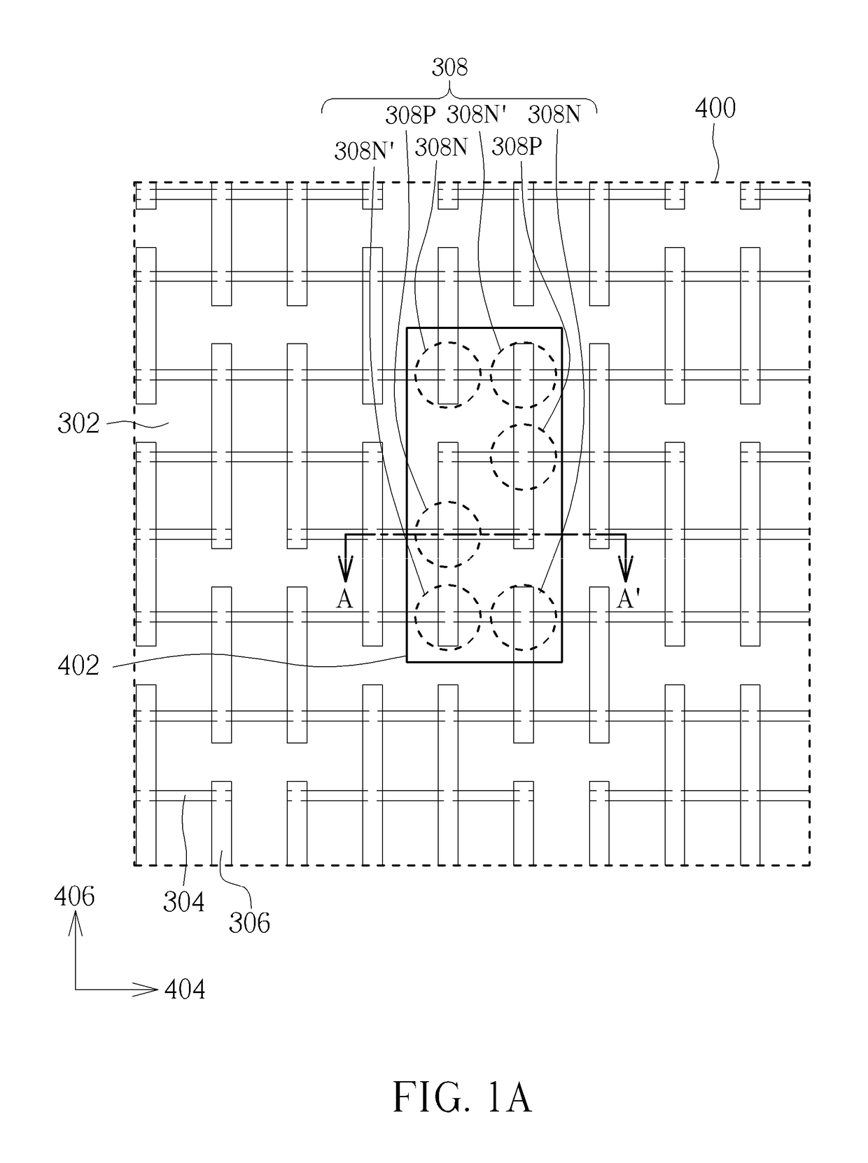
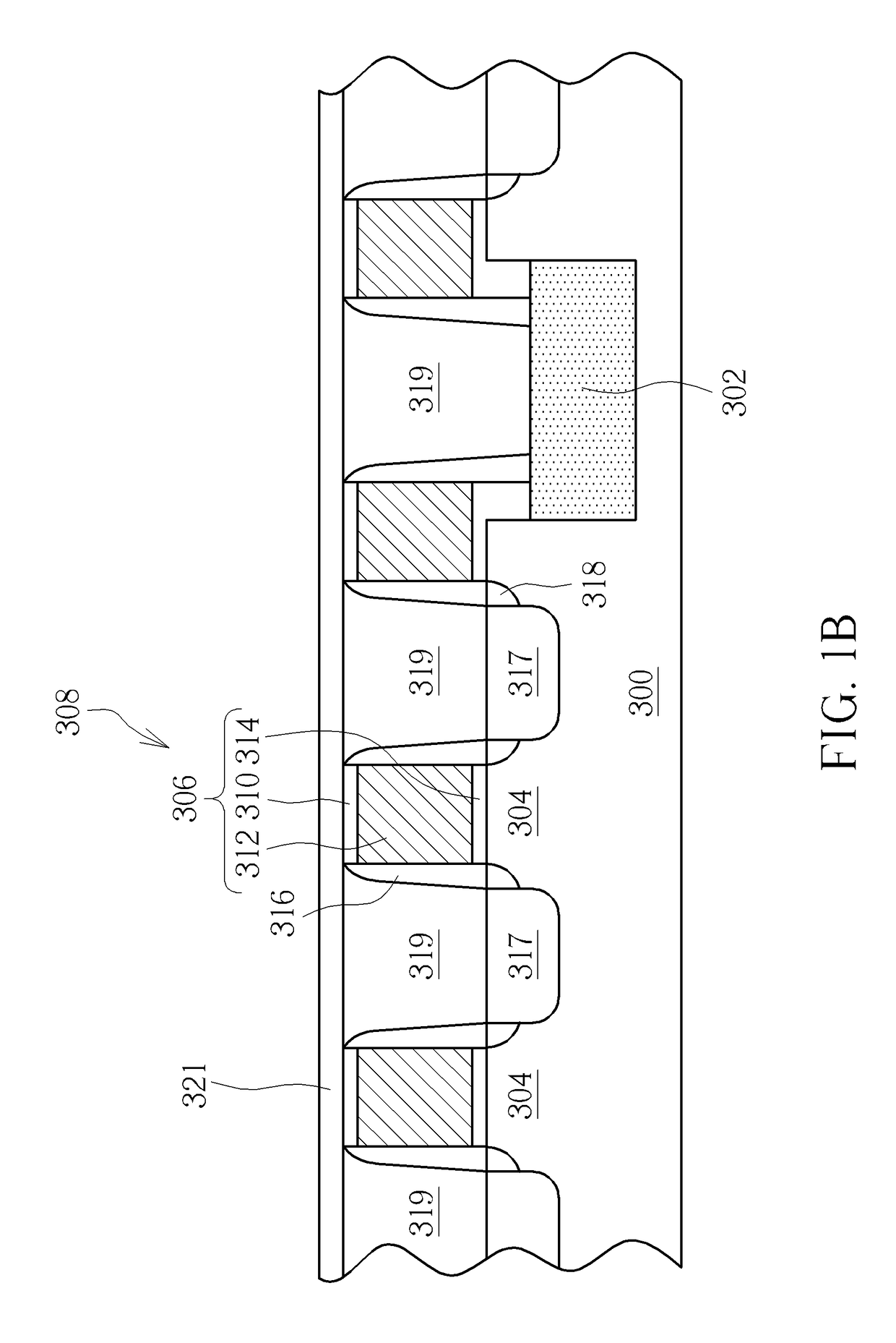
[0017]Please see FIG. 1A, FIG. 1B, FIG. 2A, FIG. 2B, FIG. 3A, FIG. 3B, FIG. 4A and FIG. 4B showing schematic diagrams of the method for forming the semiconductor device according to the one embodiment of the present invention, wherein FIG. 1A, FIG. 2A, FIG. 3A, FIG. 4A are top view, and FIG. 1B, FIG. 2B, FIG. 3B, FIG. 4B are cross-sectional view taken along line QQ′ of FIG. 1A, FIG. 2A, FIG. 3A, FIG. 4A, FIG. 5A, respectively.

[0018]Please see FIG. 1A and FIG. 1B first. A substrate 300 is provided to serve as a base for forming devices, components, or circuits. The substrate 300 is preferably composed of a silicon containing material. Silicon containing materials include, but are not limited to, Si, single crystal Si, polycrystalline Si, SiGe, single crystal si...


PUM


Abstract

The present invention provides a semiconductor structure, including a substrate, a plurality of fin structures, a plurality of gate structures, a dielectric layer and a plurality of contact plugs. The substrate has a memory region. The fin structures are disposed on the substrate in the memory region, each of which stretches along a first direction. The gate structures are disposed on the fin structures, each of which stretches along a second direction. The dielectric layer is disposed on the gate structures and the fin structures. The contact plugs are disposed in the dielectric layer and electrically connected to a source / drain region in the fin structure. From a top view, the contact plug has a trapezoid shape or a pentagon shape. The present invention further provides a method for forming the same.

Description

BACKGROUND OF THE INVENTION[0001]1. Field of the Invention[0002]The present invention is related to a semiconductor structure and a method of forming of the same, and more particularly, to a semiconductor structure having contact plugs and a method of forming the same.[0003]2. Description of the Prior Art[0004]In recent years, as various kinds of consumer electronic products have been constantly developed towards miniaturization and the size of semiconductor components has reduced accordingly, in order to meet requirements of high integration, high performance, low power consumption, and demands for the products.[0005]However, with the miniaturization development of the electronic products, current planar transistors no longer meet the requirements of the products. Non-planar transistors, such as fin field effect transistors (Fin-FET), have been therefore to obtain a high drive current and to lessen short channel effect. However, due to the three-dimensional structure of the Fin-FET...

Claims


Application Information

Patent Timeline
Patent Type & Authority Patents(United States)
IPC IPC(8): H01L27/11H01L29/76H01L21/768H01L29/78H01L23/535H01L21/8234H01L21/311
CPCH01L27/1108H01L21/31144H01L21/76802H01L21/76877H01L21/823431H01L21/823475H01L23/535H01L29/7851H01L23/485H01L21/76897H01L27/0924H01L21/823821H10B10/12H10B10/125H01L21/76805H01L21/76895H01L21/823871H01L27/0922H01L29/7853
Inventor HUNG, CHING-WENLO, WEI-CYUANCHEN, MING-JUILU, CHIA-LINWU, JIA-RONGLEE, YI-HUILIU, YING-CHENGWU, YI-KUANHUANG, CHIH-SENCHEN, YI-WEIYIN, TAN-YAHUANG, CHIA-WEIWANG, SHU-RUCHENG, YUNG-FENG
Owner UNITED MICROELECTRONICS CORP
Why Eureka
Try Eureka