
IGBT manufacturing method

a manufacturing method and technology of igbt, applied in the direction of transistors, semiconductor devices, electrical apparatus, etc., can solve the problems of fatal damage to the electrical parameter and the yield of the device, relative more defects on the epitaxial layer, and difficulty in consistency of thickness and specific resistance, so as to reduce the performance of the device and reduce the surface defects of the substrate material. , the effect of reducing the defect ra

Active Publication Date: 2017-04-11
CSMC TECH FAB2 CO LTD
View PDF13 Cites 4 Cited by
  • Summary
  • Abstract
  • Description
  • Claims
  • Application Information

AI Technical Summary

Benefits of technology

The patent discusses a problem in the manufacturing of low voltage IGBTs. The process can result in surface defects on the substrate material, which negatively impact the quality of the epitaxial layer and the overall performance of the device. To address this issue, the patent provides an IGBT manufacturing method that improves the quality of the substrate material before epitaxy, resulting in a higher quality epitaxial layer and ultimately a better performing device.

Problems solved by technology

For a normal low voltage IGBT, especially for FS-IGBT manufactured by an epitaxy technology at about 600 volts, the technology difficult is the consistency of the thickness and the specific resistance.
However, the silicon wafer grown by the low voltage epitaxy technology has a great temperature gradient which results to a great deal of stacking fault and dislocation, a great stacking fault density and a dislocation density will bring a fatal damage to the electrical parameter and the yield of the device.
Thus, for the normal P-type substrate, because the injection is done before the epitaxy technology and the substrate material has relative more surface defects, results in relative more defects on the epitaxial layer, and the epitaxy quality is poor, causing the product to have performance problems.
In such manufacturing technology, because the injection is done before the epitaxy technology and the substrate material has relative more surface defects, results in relative more defects on the epitaxial layer, and the epitaxy quality is poor, causing the product to have obvious defects such as performance problems.
Secondly, the growth rate of the silicon epitaxy changes according to a change of the silicon source concentration.
However, when the diameter of the substrate becomes greater, because the substrate material has relative more surface defects, causing such difference to be greater which goes beyond the tolerance range in production.

Method used


Image

  • IGBT manufacturing method
  • IGBT manufacturing method
  • IGBT manufacturing method

Examples


Embodiment Construction

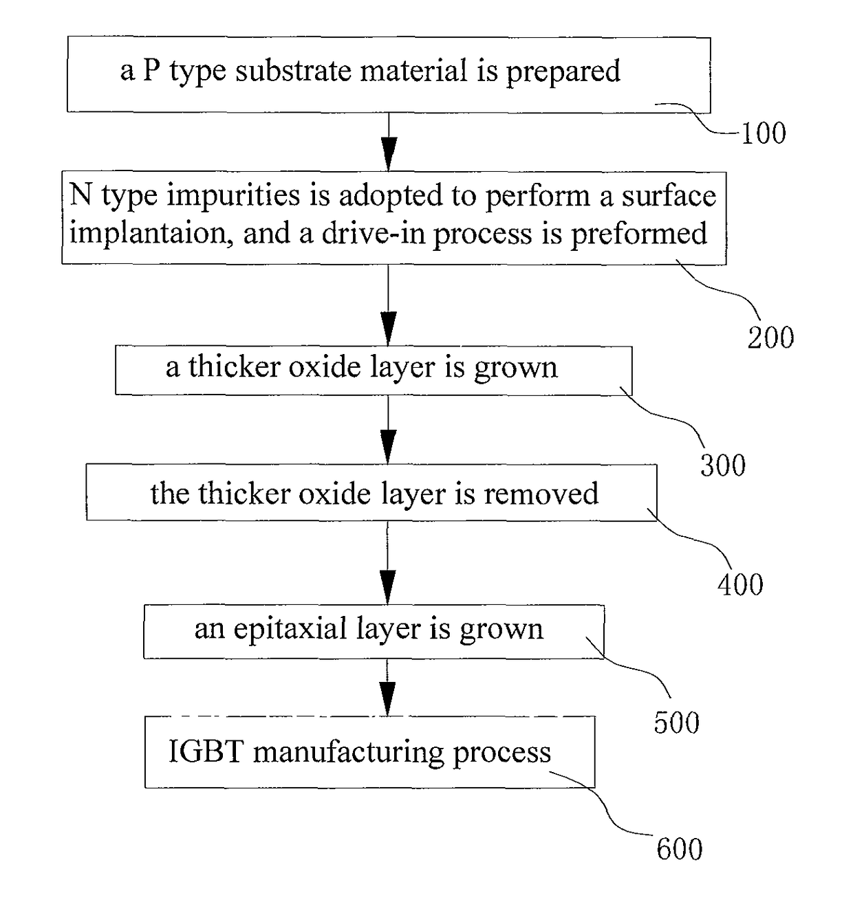
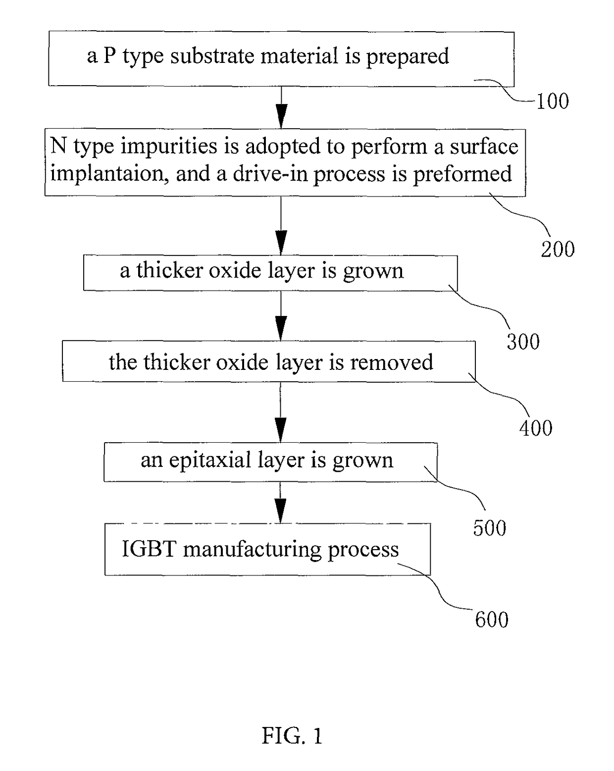
[0017]For the purpose of better understanding the above objects, features and advantages, embodiments of the present invention will be described in detail hereinafter in conjunction with the drawings.

[0018]To facilitate the sufficient understanding of the invention, many details are set forth in the following description. However, the present invention may be implemented in other manners than those described herein, and similar extensions may be made by those skilled in the art without deviating from the spirit of the present invention. Therefore, the present invention is not limited by the embodiments disclosed hereinafter.

[0019]Furthermore, the present invention is described in detail in conjunction with simplified cross sectional views. In describing the embodiments of the present invention in detail, for convenient description, sectional views showing structures of the device are not drawn to scale, and these simplified cross sectional views are only examples and should not limi...


PUM


Abstract

An insulated gate bipolar transistor (IGBT) manufacturing method comprises the following steps: providing a semiconductor substrate of a first conducting type, the semiconductor substrate having a first major surface and a second major surface (100); forming a field-stop layer of a second conducting type on the first major surface of the semiconductor substrate (200); growing an oxide layer on the field-stop layer (300); removing the oxide layer from the field-stop layer (400); forming an epitaxial layer on the field-stop layer from which the oxide layer has been removed; and then manufacturing an IGBT on the epitaxial layer (600). Before regular manufacturing of an IGBT, the surface defects of a substrate material are eliminated as many as possible before epitaxy is formed, and the quality of an epitaxial layer is improved, thereby improving the quality of the whole IGBT.

Description

FIELD OF THE INVENTION[0001]The invention relates to an IGBT (Insulated Gate Bipolar Transistor) in the technical field of power semiconductor device, and more particularly, relates to a manufacturing method for FS-IGBT (Field Stop Insulated Gate Bipolar Transistor) via an epitaxy technology.BACKGROUND OF THE INVENTION[0002]As the rapid development of the integrated circuit, a more exact requirement directed to a quality of the substrate material is required. For a normal low voltage IGBT, especially for FS-IGBT manufactured by an epitaxy technology at about 600 volts, the technology difficult is the consistency of the thickness and the specific resistance. The major reason of a low consistency of the specific resistance is an auto-dope of the boron impurity and arsenic impurity. Auto-dope of the N-type impurities (arsenic or phosphorus) can be eliminated by adopting a low voltage epitaxy technology. However, the silicon wafer grown by the low voltage epitaxy technology has a great ...

Claims


Application Information

Patent Timeline
Patent Type & Authority Patents(United States)
IPC IPC(8): H01L21/00H01L21/311H01L29/06H01L21/265H01L29/66H01L29/739
CPCH01L29/66333H01L21/26513H01L21/31111H01L29/0611H01L29/7395H01L29/66325
Inventor DENG, XIAOSHERUI, QIANGZHANG, SHUOWANG, GENYI
Owner CSMC TECH FAB2 CO LTD
Learn More