Silicon carbide field effect transistor

a field effect transistor and silicon carbide technology, applied in the direction of transistors, semiconductor devices, electrical equipment, etc., can solve the problems of limitations in the depth of the deep trench doped region, and achieve the effect of enhancing the reliability of the silicon carbide field effect transistor and reducing the electric field

Active Publication Date: 2017-06-20
SHANGHAI HESTIA POWER INC
View PDF11 Cites 0 Cited by
  • Summary
  • Abstract
  • Description
  • Claims
  • Application Information

AI Technical Summary

Benefits of technology

[0009]In the n-type drift layer of the present invention, the second doped blocks are arranged at an interval from the first doped block towards the silicon carbide substrate. Further, a thickness of the second doped blocks does not exceed 2 um. Accordingly, not only the issue of limitations posed by the energy of ion implantation and the thickness of the hard mask layer is solved, but also power lines are effectively dispersed to reduce the electric field at the bottom and the corner of the trench gate, thereby enhancing the reliability of the silicon carbide field effect transistor.

Problems solved by technology

However, a doped depth of the deep trench doped region suffers from limitations posed by an energy of ion implantation and a thickness of a hard mask layer.

Method used


Image

  • Silicon carbide field effect transistor
  • Silicon carbide field effect transistor
  • Silicon carbide field effect transistor

Examples


Embodiment Construction

[0012]The foregoing, as well as additional objects, features and advantages of the invention will be more readily apparent from the following detailed description, which proceeds with reference to the accompanying drawings.

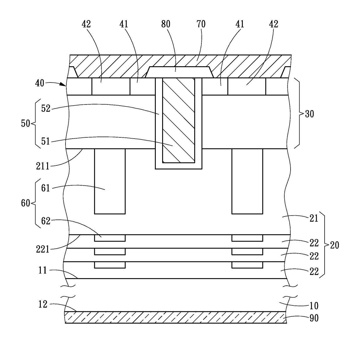
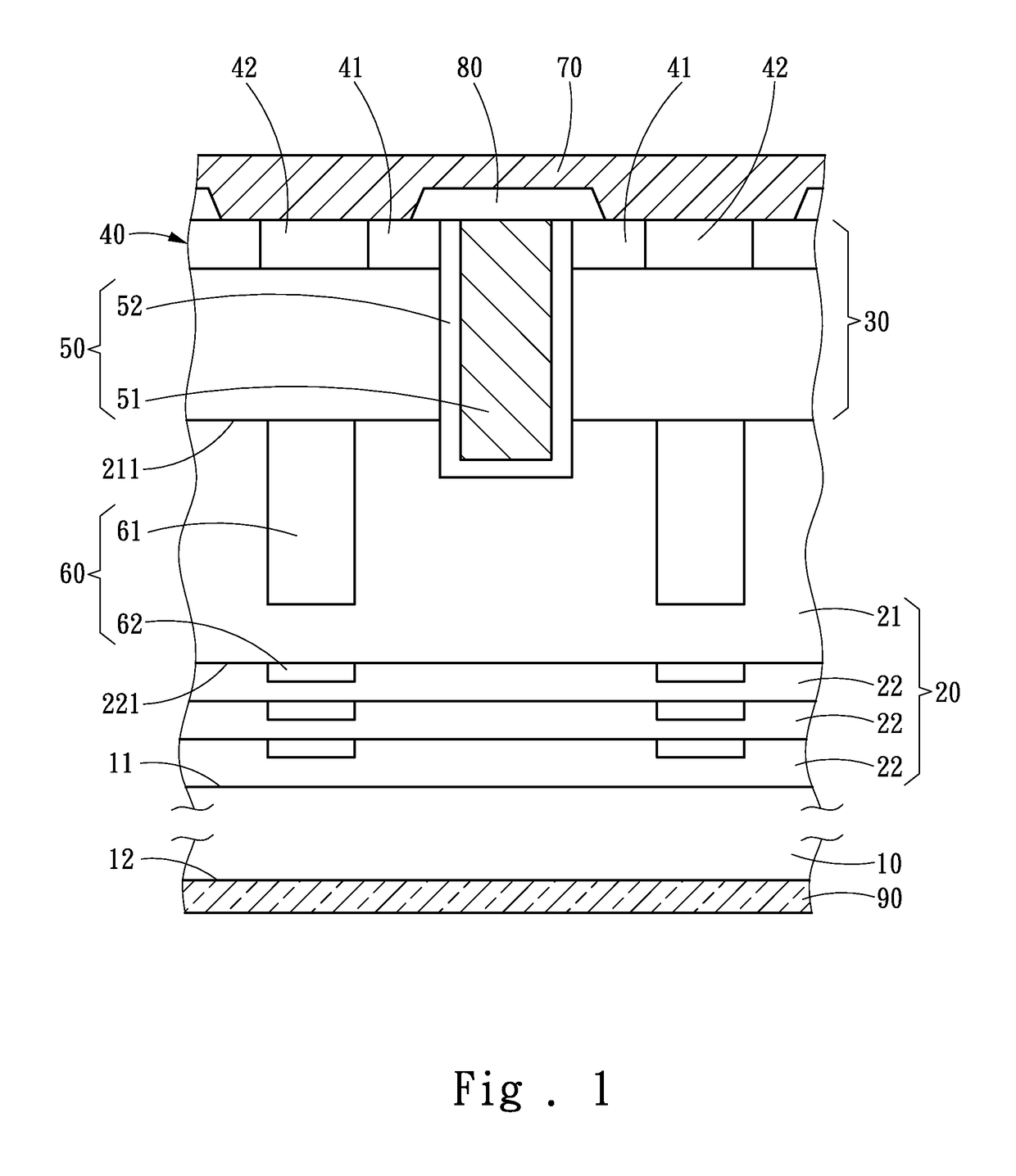
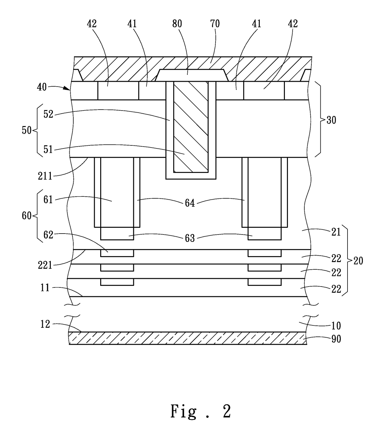
[0013]FIG. 1 shows a schematic diagram of a structure according to a first embodiment of the present invention. A silicon carbide field effect transistor provided by the present invention includes a silicon carbide substrate 10, an n-type drift layer 20, a p-type epitaxy layer 30, a source region 40, a trench gate 50, at least one p-type doped region 60, a source 70, a dielectric layer 80 and a drain 90.

[0014]The silicon carbide substrate 10 may be obtained by cutting crystalline silicon carbide into a predetermined thickness or by forming crystalline silicon carbide on any substrate, or may be a commercial silicon carbide substrate 10. Given a substrate having a surface formed with crystalline silicon carbide is utilized, the type of silicon carbide substrate is ...


PUM


Abstract

A silicon carbide field effect transistor includes a silicon carbide substrate, an n-type drift layer, a p-type epitaxy layer, a source region, a trench gate, at least one p-type doped region, a source, a dielectric layer and a drain. The p-type doped region is disposed at the n-type drift layer to be adjacent to one lateral side of the trench gate, and includes a first doped block and a plurality of second doped blocks arranged at an interval from the first doped block towards the silicon carbide substrate. Further, a thickness of the second doped blocks does not exceed 2 um. Accordingly, not only the issue of limitations posed by the energy of ion implantation is solved, but also an electric field at a bottom and a corner of the trench gate is effectively reduced, thereby enhancing the reliability of the silicon carbide field effect transistor.

Description

FIELD OF THE INVENTION[0001]The present invention relates to a semiconductor device, and particularly to a silicon carbide field effect transistor.BACKGROUND OF THE INVENTION[0002]The breakdown voltage, one of the characteristics of a semiconductor power device, is designed towards targets of having a minimal conduction resistance, a low reverse leakage current and a fast switching speed, so as to reduce a conduction loss as well as switching loss. Having a wide bandgap (Eg=3.26 eV), a high threshold breakdown strength (2.2 MV / cm) and a high thermal conductivity (4.9 W / cm-K), silicon carbide (SiC) is regarded as an ideal material for power switching devices. Therefore, many associated industrialist are dedicated in the development and research of silicon carbide power devices.[0003]For example, the U.S. patent publication No. US2013 / 0161736 discloses a trench metal oxide semiconductor transistor device and manufacturing method thereof The trench metal includes a substrate of a first...

Claims


Application Information

Patent Timeline
Patent Type & Authority Patents(United States)
IPC IPC(8): H01L29/78H01L29/08H01L29/66H01L21/04H01L29/423H01L29/16H01L29/10
CPCH01L29/7813H01L21/046H01L29/086H01L29/0865H01L29/1095H01L29/1608H01L29/4236H01L29/66068H01L29/0623H01L29/0634H01L29/0649
Inventor HUNG, CHIEN-CHUNGYEN, CHENG-TYNGHUNG, HSIANG-TINGLEE, CHWAN-YING
Owner SHANGHAI HESTIA POWER INC
Why Eureka
Try Eureka