Solid-state image sensor and imaging apparatus including the same

a solid-state image sensor and imaging apparatus technology, applied in the field of large-form-factor solid-state image sensors and imaging apparatuses, can solve the problems of limiting the size of the silicon wafer used for the available image unable to capture motion pictures without image lag, and difficult or alternatively, to use an optical lens system for refracting x-rays, etc., to prevent or limit radiation damage, reduce the size of the silicon wafer, and reduce the size of the mos sensor

Active Publication Date: 2017-11-07
SHIZUKUISHI MAKOTO
View PDF55 Cites 4 Cited by
  • Summary
  • Abstract
  • Description
  • Claims
  • Application Information

AI Technical Summary

Benefits of technology

[0018]Example embodiments provide a MOS sensor and an X-ray system including the same. Example embodiments provide a MOS sensor that has a relatively large image sensing area and is capable of motion picture imaging with relatively low image lag. In addition, example embodiments further provide a MOS sensor that includes little or no dead space on the sensor surface. Example embodiments still further provide a MOS sensor having a curved surface. In addition, example embodiments provide a MOS sensor that is capable of preventing or limiting radiation damage.

Problems solved by technology

Unlike a visible light image sensor, it may be difficult or, alternatively, impossible to use an optical lens system for refracting X-rays.
However, it may be difficult for the conventional X-ray image sensors to capture a motion picture without image lag due to the large capacitive load and the TFT's slow switching speed.
The available image size of the MOS sensor, however, may be limited by the size of a silicon wafer used.
Straight and same pitch global lines may be routed with the pixel array and such routing may suppress fixed pattern noise due to signal delay non-uniformity.
However, a hooked or L-shaped semiconductor chip may be difficult for a wafer dicing machine to cut or form.
It should be also noted that the semiconductor chip may be damaged by high energy particles or radiation like X-ray beam.
This shift in threshold voltages may cause image quality of the MOS image sensor to deteriorate and eventually reduce a product life time of the MOS image sensor.

Method used


Image

  • Solid-state image sensor and imaging apparatus including the same
  • Solid-state image sensor and imaging apparatus including the same
  • Solid-state image sensor and imaging apparatus including the same

Examples


Embodiment Construction

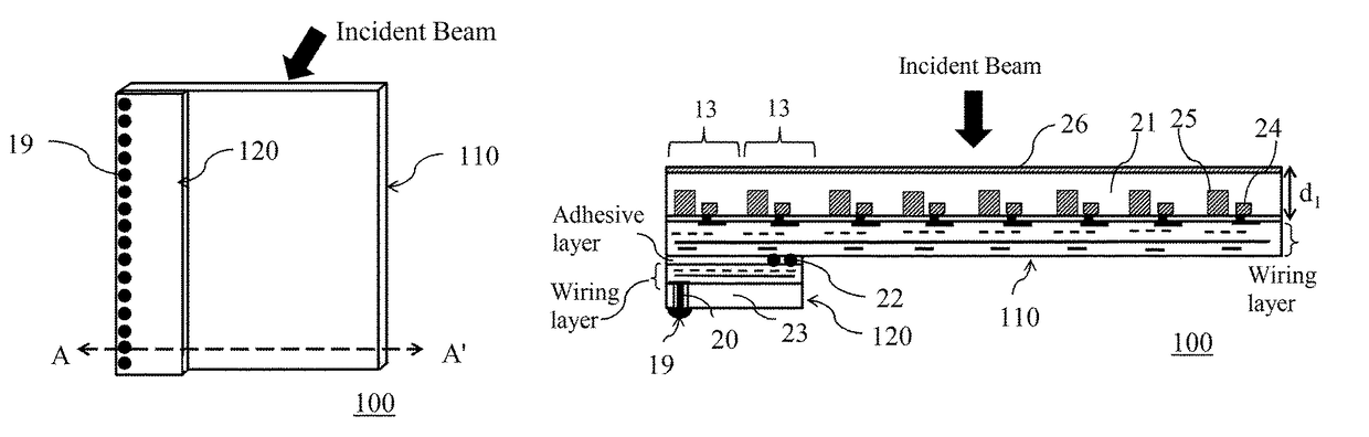
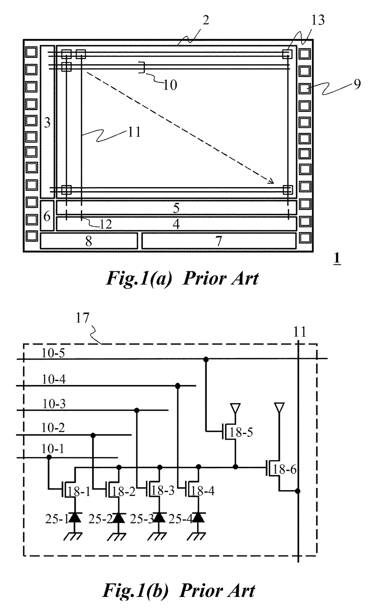
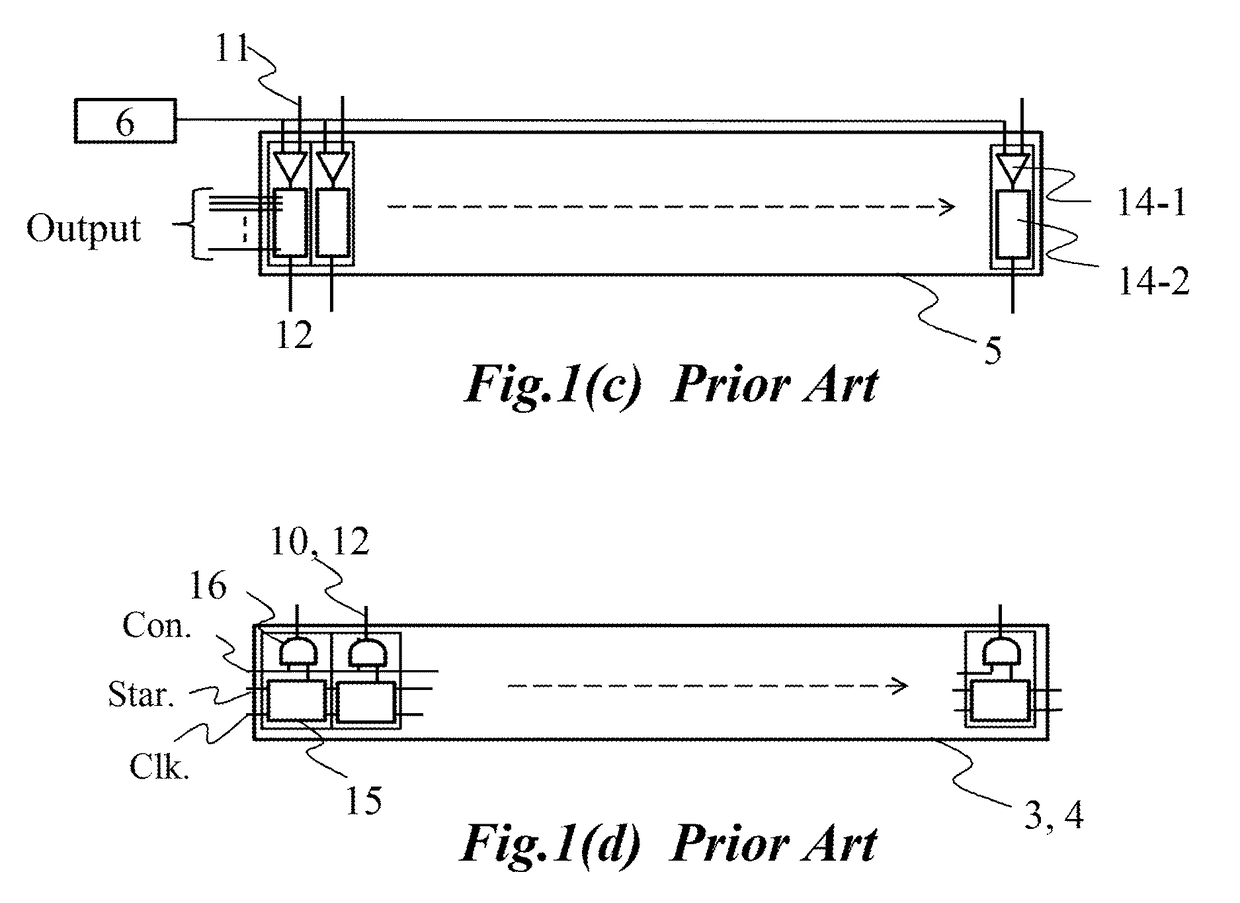
[0062]Detailed example embodiments are disclosed herein. However, specific structural and functional details disclosed herein are merely representative for purposes of describing example embodiments. Example embodiments may, however, be embodied in many alternate forms and should not be construed as limited to only the embodiments set forth herein.

[0063]Accordingly, while example embodiments are capable of various modifications and alternative forms, embodiments thereof are shown by way of example in the drawings and will herein be described in detail. It should be understood, however, that there is no intent to limit example embodiments to the particular forms disclosed, but to the contrary, example embodiments are to cover all modifications, equivalents, and alternatives falling within the scope of example embodiments. Like numbers refer to like elements throughout the description of the figures.

[0064]It will be understood that, although the terms first, second, etc. may be used h...


PUM


Abstract

An image sensor includes a first semiconductor chip including first and second surfaces; a second semiconductor chip including first and second surfaces; and a first adhesive layer between the second surface of the first semiconductor chip and the second surface of the second semiconductor chip, the first semiconductor chip being stacked on the second semiconductor chip via the first adhesive layer such that a footprint of the first semiconductor chip is larger than a footprint of the second semiconductor chip with respect to a plan view of the image sensor, the first semiconductor chip including an array of unit pixels configured to capture light corresponding to an image and to generate image signals based on the captured light, the second semiconductor chip including first peripheral circuits configured to control the array of unit pixels and receive the generated image signals.

Description

CROSS-REFERENCE TO RELATED APPLICATION[0001]This application claims priority under 35 U.S.C. §119 to Japanese Patent Application No. 2013-098454 filed on May 8, 2013, in the Japanese Patent Office (JPO), the entire contents of which are incorporated herein by reference.BACKGROUND[0002]1. Technical Field[0003]Example embodiments relate to a large form factor solid state image sensor and an imaging apparatus using the same.[0004]2. Related Art[0005]Solid-state image sensors may be applied to medical instruments in order to enable the use of the medical instruments for discovering a disease or other condition harmful to the health of a patient in the early stages of the condition thereby reducing medical expenses. X-ray imaging systems may be used for this purpose.[0006]Unlike a visible light image sensor, it may be difficult or, alternatively, impossible to use an optical lens system for refracting X-rays. Instead it may be desirable to use a large image size sensor or tiled image sen...

Claims


Application Information

Patent Timeline
Patent Type & Authority Patents(United States)
IPC IPC(8): A61B6/00A61B5/00H01L27/146G01T1/24
CPCA61B5/0062A61B5/0035A61B5/0077A61B6/4233H01L27/14661H01L27/14676G01T1/243H01L27/14634A61B6/4266
Inventor SHIZUKUISHI, MAKOTO
Owner SHIZUKUISHI MAKOTO
Why Eureka
Try Eureka