Unlock instant, AI-driven research and patent intelligence for your innovation.

Periodic table group 13 metal nitride crystals and method for manufacturing periodic table group 13 metal nitride crystals

a metal nitride crystal and periodic table technology, applied in the direction of crystal growth process, polycrystalline material growth, chemically reactive gas, etc., can solve the problems of inability to provide periodic table large-scale, inability to obtain large-scale substrates, and inability to provide conventional methods, etc., to achieve easy production, low cost, and low cost

Active Publication Date: 2017-12-12
MITSUBISHI CHEM CORP
View PDF20 Cites 0 Cited by
  • Summary
  • Abstract
  • Description
  • Claims
  • Application Information

AI Technical Summary

Benefits of technology

This approach enables the production of high-quality, large-size Group 13 metal nitride crystals with reduced stacking faults, leading to improved light-emitting devices with enhanced efficiency and durability by suppressing stacking faults, particularly in directions parallel to polar planes.

Problems solved by technology

As described above, although a method which homoepitaxially grows a crystal on a periodic table Group 13 metal nitride seed in which a polar plane serves as the principal plane, then cuts the crystal so that a desired plane emerges is able to obtain a periodic table Group 13 metal nitride substrate having few stacking faults, a large-size substrate cannot be obtained.
In this way, it has not been possible with conventional methods to provide periodic table Group 13 metal nitride crystals which have few stacking faults and are moreover large in size.
However, no methods for providing such periodic table Group 13 metal nitride crystals have hitherto been proposed.

Method used


Image

  • Periodic table group 13 metal nitride crystals and method for manufacturing periodic table group 13 metal nitride crystals
  • Periodic table group 13 metal nitride crystals and method for manufacturing periodic table group 13 metal nitride crystals
  • Periodic table group 13 metal nitride crystals and method for manufacturing periodic table group 13 metal nitride crystals

Examples


examples 3 to 7

[0183]In each of these examples, aside from changing the misorientation angle of the principal plane in the [000-1] direction and the growth temperature to the conditions indicated in Table 1, a GaN bulk crystal was obtained in the same way as in Example 2. The crystal grown on the underlying substrate had an average film thickness in the [10-10] direction of about 1 mm. The results are presented in Table 1.

[0184]

TABLE 1Example 2Example 3Example 4Example 5Example 6Example 7UnderlyingUnderlying substrateGaNGaNGaNGaNGaNGaNsubstrateOrientation of principal plane(10-10)(10-10)(10-10)(10-10)(10-10)(10-10)Misorientation angle of principal123512Plane in -c-axis direction (°)GaN layerGrowth temperature (° C.)95095095095010001000Growth rate (μm / hr)767575776968LTPL intensity ratio (I(BSF) / I(D0XA)0.080.030.040.080.110.04Presence / absence of cracksNo cracksNo cracksNo cracksNo cracksNo cracksNo cracks

[0185]The stacking fault densities of the GaN bulk crystals obtained were evaluated by low-tempe...

example 8

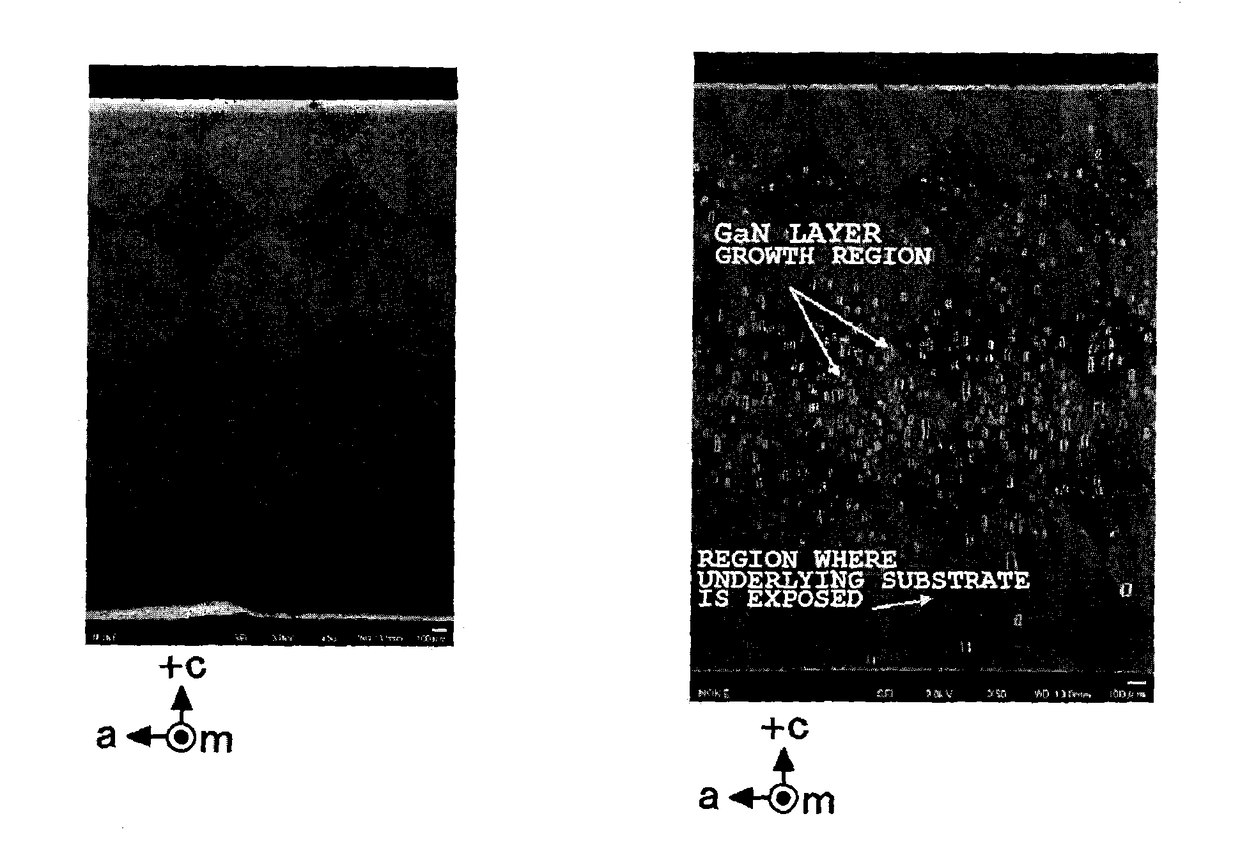
[0192]Crystal growth was carried out using a HVPE crystal manufacturing apparatus. A total of 22 GaN self-supporting substrates were manufactured by (0001) plane growth. Each was of a rectangular shape measuring 5 mm in the (c-axis) direction and 30 mm in the (a-axis direction), and had a principal plane that was tilted 2° in the [000-1] direction from the (10-10) plane. The 22 substrates were arranged in two rows in the (c-axis) direction and 11 rows in the (a-axis) direction, and placed on a susceptor. The susceptor on which the arranged substrates had been mounted was placed in the reactor, the temperature of the periodic table Group 13 source reservoir 106 was raised to 900° C. and the temperature of the reaction chamber was raised to the growth temperature of 950° C., and a GaN single-crystal layer was grown by HVPE for 53 hours. In this single-crystal growth step, the growth pressure was set to 1.01×10⁵ Pa, the partial pressure of GaCl gas was set to 3.54×10² Pa, the parti...

example 9

rowth Using Seed Crystal in which Substrate Sidewall is Semi-Polar Plane

(Production of Seed Crystal)

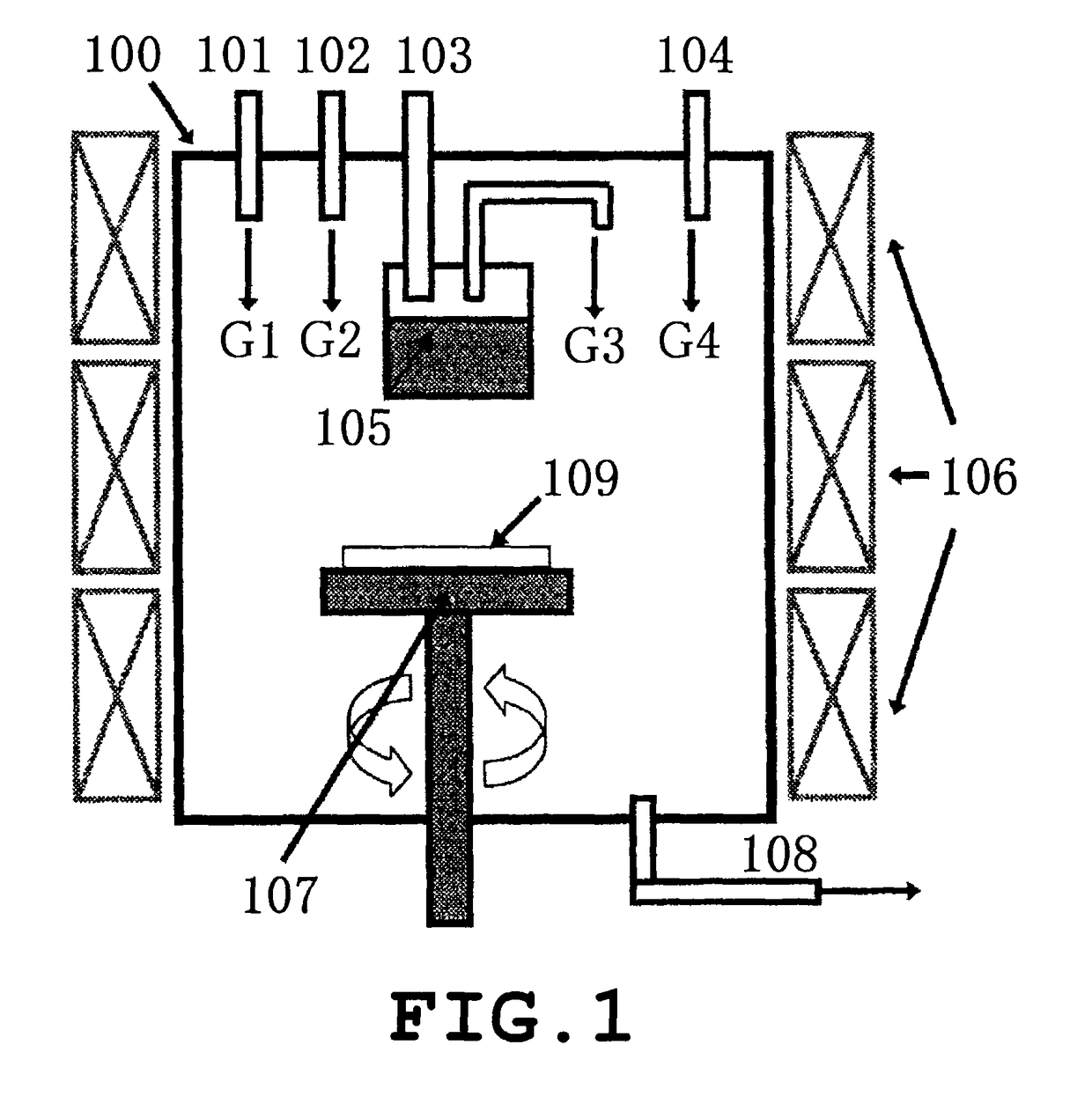
[0198]Crystal growth was carried out using the HVPE crystal manufacturing apparatus shown in FIG. 1. A total of 33 GaN self-supporting substrates 1′ were manufactured by (0001) plane growth. Each was of a rectangular shape measuring 5 mm in the (c-axis) direction and 25 mm in the (a-axis direction), and had a principal plane that was the (10-10) plane. The 33 substrates were arranged in three rows in the (c-axis) direction and 11 rows in the (a-axis) direction, and placed on a susceptor 107. The susceptor 107 with the arranged substrates loaded thereon was placed in a reactor 100 as shown in FIG. 1, the temperature of the reaction chamber was raised to 1000° C., and a GaN single-crystal film was grown for 40 hours by the HVPE process. In this single-crystal growth step, the growth pressure was set to 1.01×10⁵ Pa, the partial pressure of GaCl gas was set to 3.70×10² Pa, the partial...


PUM

PropertyMeasurementUnit
thicknessaaaaaaaaaa
misorientation angle distributionaaaaaaaaaa
thicknessaaaaaaaaaa

Abstract

A periodic table Group 13 metal nitride crystals grown with a non-polar or semi-polar principal surface have numerous stacking faults. The purpose of the present invention is to provide a period table Group 13 metal nitride crystal wherein the occurrence of stacking faults of this kind are suppressed. The present invention achieves the foregoing by a periodic table Group 13 metal nitride crystal being characterized in that, in a Qx direction intensity profile that includes a maximum intensity and is derived from an isointensity contour plot obtained by x-ray reciprocal lattice mapping of (100) plane of the periodic table Group 13 metal nitride crystal, a Qx width at 1 / 300th of peak intensity is 6×10⁻⁴ rlu or less.

Description

CROSS-REFERENCE TO RELATED APPLICATION[0001]This is a continuation of International Application PCT / JP2013 / 059631, filed on Mar. 29, 2013, and designated the U.S., (and claims priority from Japanese Patent Application 2012-081735 which was filed on Mar. 30, 2012 and Japanese Patent Application 2012-082153 which was filed on Mar. 30, 2012,) the entire contents of which are incorporated herein by reference.TECHNICAL FIELD[0002]The present invention relates to a periodic table Group 13 metal nitride crystal and to a method of manufacturing a periodic table Group 13 metal nitride crystal. The invention relates in particular to a periodic table Group 13 metal nitride crystal in which the occurrence of stacking faults is suppressed and to a method of manufacturing such a crystal.BACKGROUND ART[0003]A nitride semiconductor represented by gallium nitride has large band gap, and interband transition is a direct transition. Therefore, the nitride semiconductor is a useful material for light e...

Claims


Application Information

Patent Timeline
Patent Type & Authority Patents(United States)
IPC IPC(8): C30B29/40H01L21/02H01L29/20C30B25/14C30B25/20C30B25/02
CPCC30B29/406C30B25/02C30B25/14C30B25/20C30B29/403H01L29/2003H01L21/0262H01L21/02389H01L21/02433H01L21/02634H01L21/0254
Inventor ENATSU, YUUKINAGAO, SATORUKUBO, SHUICHIIKEDA, HIROTAKAFUJITO, KENJI
Owner MITSUBISHI CHEM CORP