Low temperature formation of high quality silicon oxide films in semiconductor device manufacturing

a technology of silicon oxide film and low temperature, applied in the direction of coating, chemical vapor deposition coating, metallic material coating process, etc., can solve the problems of unacceptably high stress value of conventional low temperature pecvd and less attractive for use as hardmasks, and achieve the effect of reducing the stress of the deposited layer

Active Publication Date: 2017-12-19
LAM RES CORP
View PDF458 Cites 200 Cited by
  • Summary
  • Abstract
  • Description
  • Claims
  • Application Information

AI Technical Summary

Benefits of technology

[0011]In another aspect, a method for processing a semiconductor substrate involving UV treatment is provided. The method includes: (a) providing a semiconductor substrate to a PECVD process chamber; (b) depositing a layer of silicon oxide on the semiconductor substrate by PECVD at a temperature of less than about 200° C.; (c) stoppin

Problems solved by technology

There is currently a need to deposit silicon oxide by PECVD at low temperature because many integration schemes involve substrates having layers of temperature-sensitive materials (e.g., organic dielectrics) that cannot withstand high temperature PECVD.
However, conventional lo

Method used


Image

  • Low temperature formation of high quality silicon oxide films in semiconductor device manufacturing
  • Low temperature formation of high quality silicon oxide films in semiconductor device manufacturing
  • Low temperature formation of high quality silicon oxide films in semiconductor device manufacturing

Examples


experimental examples

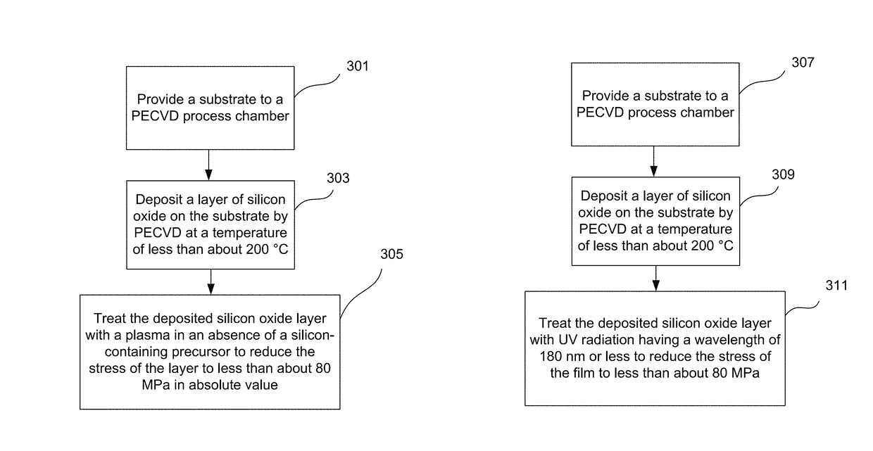
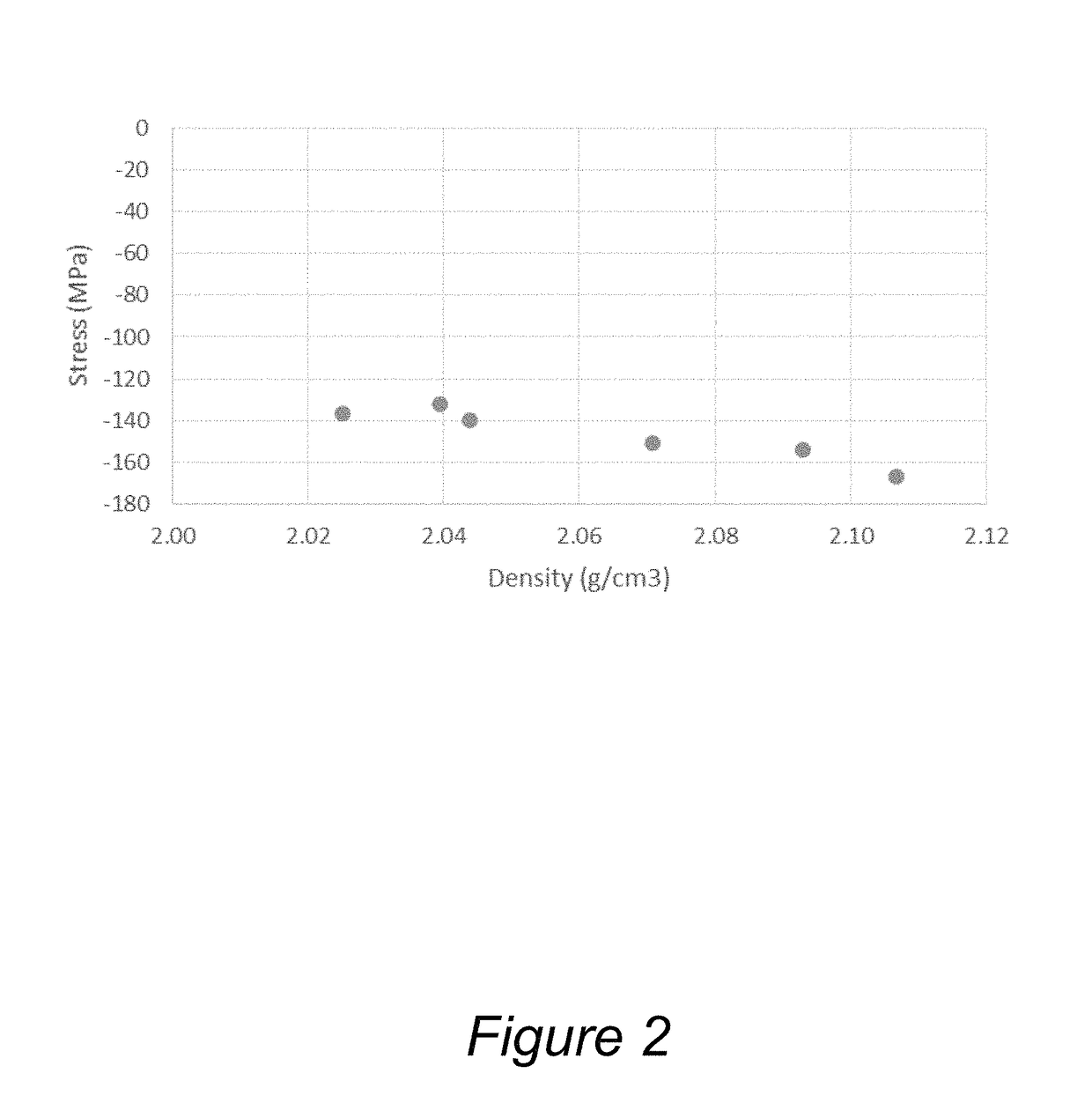
Example 1. Formation of Silicon Oxide Films Having Low Stress and High Density

[0081]A number of silicon oxide films were deposited by PECVD in a Vector PECVD reactor available from Lam Research Corporation, Fremont Calif., on planar 300 mm wafers at a temperature of 180° C., and pressures of 2.5 Torr-3.5 Torr. The process gas used during deposition consisted of SiH4 (provided at 30 sccm), CO2 (provided at 4200 sccm) and He. Plasma was generated in the process gas using HF RF generation at 13.56 MHz at a power level of 100-400 W. The deposition was conducted for 5 seconds; then the flows of SiH4 and CO2 into the process chamber were stopped, while the plasma and helium flow remained on for 5 seconds to purge the SiH4 and CO2 out of the process chamber. Next, plasma power was increased to 500-1000 W and helium flow was increased to 1000-4000 sccm and the deposited silicon oxide films were plasma treated under these conditions for 6-20 seconds. Temperature and pressure remained constan...

example 2

of Formed Low-Stress Films

[0082]An FT IR spectrum of a low-stress silicon oxide material was obtained. The film was formed as described in Example 1, using the following process parameters: temperature of 180° C., pressure of 3.5 Torr, plasma power of 100 W (generated at 13.56 Mhz), SiH4 flow rate of 30 sccm, CO2 flow rate of 4200 sccm and He flow rate of 1250 sccm. The formed film had a stress of less than −40 MPa. It can be seen that the FT IR spectrum does not have a Si—H peak at about 2250 cm−1, which is typically present in silicon oxide films deposited by low temperature PECVD without plasma post-treatment. This indicates that plasma post-treatment reduces the concentration of hydrogen in the formed films.

example 3

nt of Stress, Density, and RI by Plasma Post-Treatment

[0083]A comparative silicon oxide film was deposited by low temperature PECVD to a thickness of 411 Å, and its stress, density and RI were measured. The deposition was conducted at a temperature of 180° C., and pressure of 3.5 Torr, using plasma power of 100 W (13.56 Mhz), SiH4 flow rate of 30 sccm, CO2 flow rate of 4200 sccm and He flow rate of 1250 sccm.

[0084]Another silicon oxide film was deposited by low temperature PECVD using the same process conditions as those used in the deposition of the comparative film above, and was then plasma treated at a temperature of 180° C., pressure of 3.5 Torr, using plasma power of 500 W (13.56 Mhz), and He flow rate of 1000 sccm. Stress, density, and RI of the treated film were measured.

[0085]Parameters for the comparative film and for the treated film are provided in Table 4.

[0086]

TABLE 4Improvement of stress, density, and RI upon plasma treatment.ParameterComparative FilmTreated FilmStres...


PUM

PropertyMeasurementUnit
Temperatureaaaaaaaaaa

Abstract

Silicon oxide layer is deposited on a semiconductor substrate by PECVD at a temperature of less than about 200° C. and is treated with helium plasma to reduce stress of the deposited layer to an absolute value of less than about 80 MPa. Plasma treatment reduces hydrogen content in the silicon oxide layer, and leads to low stress films that can also have high density and low roughness. In some embodiments, the film is deposited on a semiconductor substrate that contains one or more temperature-sensitive layers, such as layers of organic material or spin-on dielectric that cannot withstand temperatures of greater than 250° C. In some embodiments the silicon oxide film is deposited to a thickness of between about 100-200 Å, and is used as a hardmask layer during etching of other layers on a semiconductor substrate.

Description

FIELD OF THE INVENTION[0001]The present invention pertains to methods of forming layers of material on a semiconductor substrate. Specifically, the invention pertains to methods for forming silicon oxide layers by plasma-enhanced chemical vapor deposition (PECVD).BACKGROUND OF THE INVENTION[0002]Fabrication of semiconductor devices typically involves deposition and patterning of several layers of different materials. When several layers are deposited in a stack, stress characteristics of deposited layers become particularly important because highly stressed materials can lead to disruption in alignment of layers in a stack, buckling, delamination, and, ultimately, to patterning inaccuracy, and semiconductor device failure.[0003]Most film deposition is associated with the introduction of residual stress in the deposited film due to both extrinsic factors (e.g., thermal expansion coefficient mismatch) and / or intrinsic factors (e.g., defects and / or dislocations within lattice). The str...

Claims


Application Information

Patent Timeline
IPC IPC(8): H01L21/31H01L21/316H01L21/3105H01L21/02H01L21/027H01L21/308C23C16/40C23C16/56
CPCH01L21/02164H01L21/02274H01L21/0234H01L21/02211H01L21/0274H01L21/02348H01L21/3081H01L21/3086C23C16/402C23C16/56H01L21/31144C23C16/45523C23C16/505
Inventor MCLAUGHLIN, KEVIN M.PHARKYA, AMITREDDY, KAPU SIRISH
Owner LAM RES CORP
Why Eureka
Try Eureka