
Photomask blank

a technology of photoresist and blank, which is applied in the field of photoresist blank, can solve the problems of difficult to accurately transfer the resist pattern to the chromium-containing film, deformation of the resist pattern, damage to the resist film, etc., and achieve the effect of reducing the thickness of the photoresist film, reducing the load on the photoresist, and high etching ra

Active Publication Date: 2018-01-09
SHIN ETSU CHEM IND CO LTD
View PDF15 Cites 0 Cited by
  • Summary
  • Abstract
  • Description
  • Claims
  • Application Information

AI Technical Summary

Benefits of technology

The invention provides a photomask blank that includes a chromium-containing film with desired optical density, high etching rate, and effective reduction of photoresist film load. The chromium-containing film maintains conductivity, preventing charge buildup and ensuring high writing accuracy in EB lithography system. Additionally, the film has minimal variation of etching rate in thickness direction, leading to improved cross-sectional profile in pattern after etching and high transfer performance of the photomask pattern. The use of the photomask blank allows for fine-size photomask pattern with high accuracy, increasing productivity of photomasks and reducing pattern size on the processable substrate.

Problems solved by technology

If the chromium-containing film is dry etched with a relatively thin resist film made mask, the resist film can be damaged during the etching so that the resist pattern may be deformed.
It is then difficult to transfer the resist pattern accurately to the chromium-containing film.
The attempt to endow the photoresist or organic film with high resolution and high patterning accuracy as well as etch resistance encounters a technical barrier.
This leads to a tradeoff relationship between high resolution / patterning accuracy and etch resistance.
However, the light element-containing chromium film reduces its conductivity with the increasing content of light elements.
In this example, however, the etching rate of the metallic chromium layer is low, which means that a plurality of layers having significantly different etching rates are arranged in the thickness direction of the film.
When the film is processed by dry etching, the cross-sectional profile of a pattern is degraded due to differencial side etching, leading to a degradation of dimensional accuracy.

Method used


Image

  • Photomask blank
  • Photomask blank
  • Photomask blank

Examples


example 1

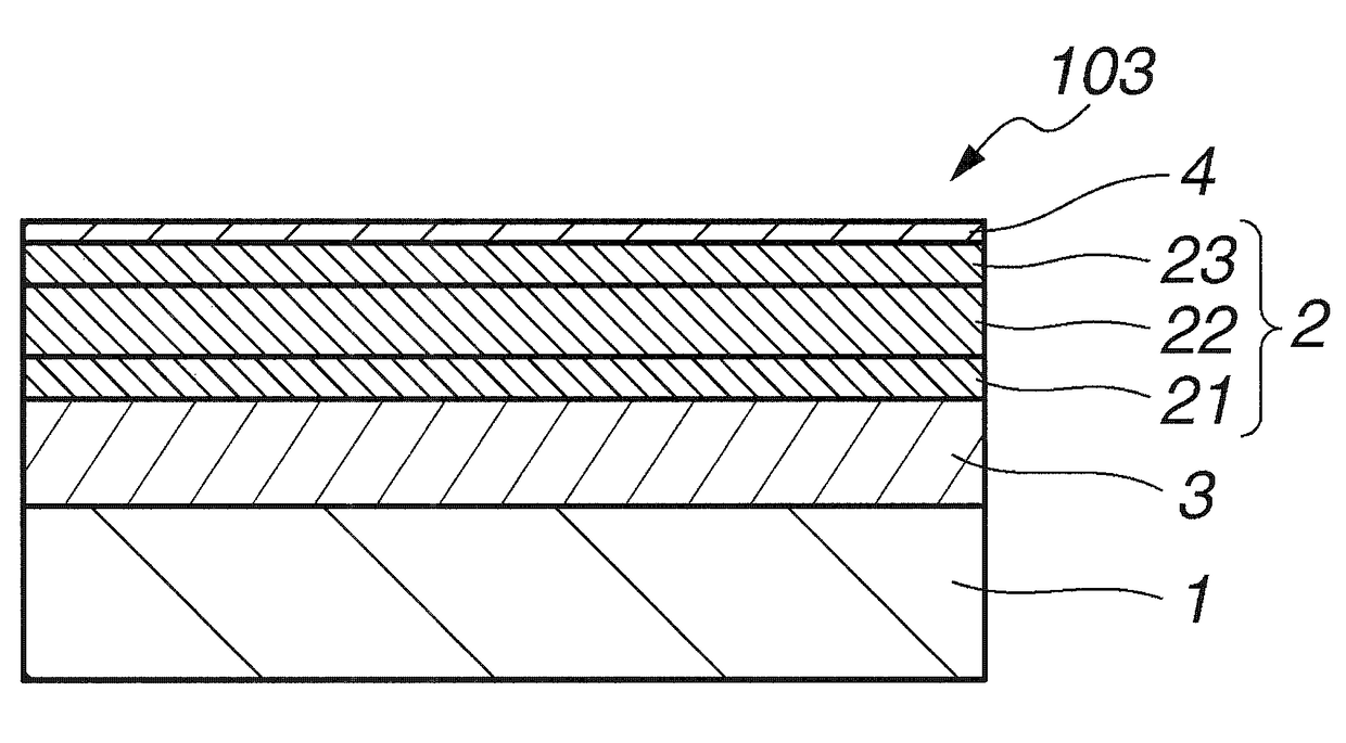
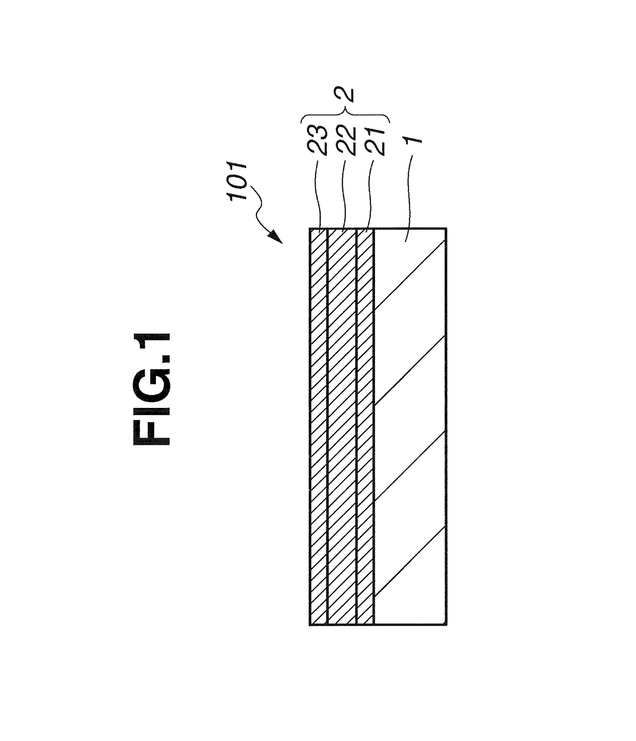
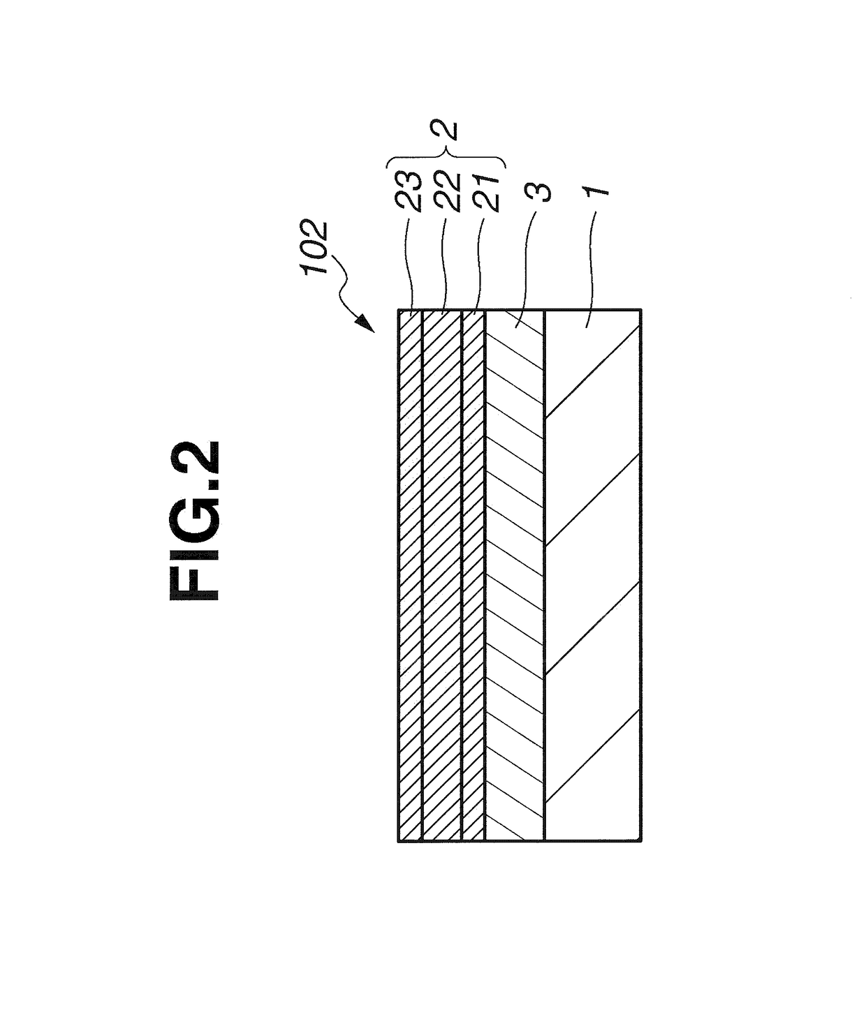
[0099]DC magnetron sputtering deposition was carried out on a quartz substrate of 152 mm squares and 6 mm thick. By sputtering a silicon target and feeding 15 sccm (flow rate) of Ar gas and 30 scorn of N2 gas as the sputtering gas into the sputtering chamber, a SiN film of 62 nm thick was deposited on the substrate as a halftone phase shift film.

[0100]DC magnetron sputtering deposition was carried out by sputtering a metallic chromium target and feeding 8 sccm of Ar gas, 25 sccm of N2 gas, and 15 sccm of O2 gas as the sputtering gas into the sputtering chamber. A CrON layer of 18 nm thick mainly functioning as an antireflective layer on the substrate side was formed on the halftone phase shift film. Next, DC magnetron sputtering deposition was carried out by sputtering a metallic chromium target and feeding 45 sccm of N2 gas as the sputtering gas into the sputtering chamber. A CrN layer of 28 nm thick mainly functioning as a conductive layer was formed. Further, DC magnetron sputter...

example 2

[0101]DC magnetron sputtering deposition was carried out on a quartz substrate of 152 mm squares and 6 mm thick. By sputtering a silicon target and feeding 15 sccm (flow rate) of Ar gas and 32 sccm of N2 gas as the sputtering gas into the sputtering chamber, a SiN film of 61 nm thick was deposited on the substrate as a halftone phase shift film.

[0102]DC magnetron sputtering deposition was carried out by sputtering a metallic chromium target and feeding 8 sccm of Ar gas, 25 sccm of N2 gas, and 15 sccm of O2 gas as the sputtering gas into the sputtering chamber. A CrON layer of 18 nm thick mainly functioning as an antireflective layer on the substrate side was formed on the halftone phase shift film. Next, DC magnetron sputtering deposition was carried out by sputtering a metallic chromium target and feeding 45 sccm of N2 gas as the sputtering gas into the sputtering chamber. A CrN layer of 23 nm thick mainly functioning as a conductive layer was formed. Further, DC magnetron sputteri...

example 3

[0103]DC magnetron sputtering deposition was carried out on a quartz substrate of 152 mm squares and 6 mm thick. By sputtering a silicon target and feeding 15 sccm (flow rate) of Ar gas and 32 seem of N2 gas as the sputtering gas into the sputtering chamber, a SiN film of 61 nm thick was deposited on the substrate as a halftone phase shift film.

[0104]DC magnetron sputtering deposition was carried out by sputtering a metallic chromium target and feeding 8 sccm of Ar gas, 25 sccm of N2 gas, and 15 sccm of O2 gas as the sputtering gas into the sputtering chamber. A CrON layer of 18 nm thick mainly functioning as an antireflective layer on the substrate side was formed on the halftone phase shift film. Next, DC magnetron sputtering deposition was carried out by sputtering a metallic chromium target and feeding 45 sccm of N2 gas and 1 sccm of O2 gas as the sputtering gas into the sputtering chamber. A CrON layer of 24 nm thick mainly functioning as a conductive layer was formed. Further,...


PUM

PropertyMeasurementUnit
optical densityaaaaaaaaaa
aspect ratioaaaaaaaaaa

Abstract

A photomask blank comprising a transparent substrate and a chromium-containing film is provided. The chromium-containing film is formed of a chromium compound containing Cr, N, and optionally O, has a total Cr+N+O content≧93 at %, and meets the formula: 3Cr≧2O+3N. A chromium compound layer meeting a first composition having a N / Cr atomic ratio≧0.95, a Cr content ≧40 at %, a Cr+N content≧80 at %, and an O content≧10 at % accounts for 10-70% of the overall thickness of the chromium-containing film.

Description

CROSS-REFERENCE TO RELATED APPLICATION[0001]This non-provisional application claims priority under 35 U.S.C. §119(a) on Patent Application No. 2015-173883 filed in Japan on Sep. 3, 2015, the entire contents of which are hereby incorporated by reference.TECHNICAL FIELD[0002]This invention relates to a photomask blank which is processed into a photomask suitable for pattern transfer using exposure light of sub-250 nm wavelength.BACKGROUND ART[0003]For goals like a higher speed of operation and a saving of power consumption of microelectronic devices, the challenge to higher integration of large-scale integrated circuits continues. To meet increasing demands for shrinkage of circuit patterns, the advanced semiconductor microprocessing technology becomes important. For example, the technology for shrinkage of circuit-constructing wiring patterns and the technology for shrinkage of contact hole patterns for cell-constructing inter-layer connections become essential.[0004]The advanced mic...

Claims


Application Information

Patent Timeline
Patent Type & Authority Patents(United States)
IPC IPC(8): G03F1/50G03F1/20G03F1/32G03F1/38G03F1/26G03F1/80
CPCG03F1/32G03F1/80G03F1/26G03F1/20G03F1/54G03F1/22G03F7/0043
Inventor SASAMOTO, KOUHEI
Owner SHIN ETSU CHEM IND CO LTD
Learn More