Silicon carbide semiconductor element and method for manufacturing the same

a silicon carbide and semiconductor element technology, applied in the field of silicon carbide semiconductor elements, can solve the problem of reducing the cross-sectional area of the configuration, and achieve the effect of reducing the conduction loss and the switching loss

Active Publication Date: 2018-03-20
PANASONIC INTELLECTUAL PROPERTY MANAGEMENT CO LTD
View PDF13 Cites 2 Cited by
  • Summary
  • Abstract
  • Description
  • Claims
  • Application Information

AI Technical Summary

Benefits of technology

[0012]The configuration, disclosed in PTL 1 enables reduction in conduction loss, because a high-concentration n-type epitaxial layer is formed. On the other hand, the n-type epitaxial layer is also formed on the JFET region. Therefore, when the semiconductor element is turned off, a spread of a depletion layer, which is expected to extend toward a substrate from the gate insulating film, is suppressed. The higher the concentration of the n-type epitaxial layer is, the smaller the extension of the depletion layer below the gate insulating film is, and the gate-drain capacitance is the highest when the extension of the depletion layer is small. That is, the high-concentration n-type epitaxial layer has an effect of reducing conduction loss, but entails an increase in the gate-drain capacitance and switching loss.
[0013]The increased gate-drain capacitance in the semiconductor element having the n-type epitaxial layer can be improved by the configuration disclosed in PTL 2, for example. However, in the configuration disclosed in PTL 2, a part of a gate electrode is removed, and thus, this configuration has a problem of decrease in the cross-sectional area where a gate current can flow by the removed area. Accordingly, from the viewpoint of a high-speed operation with low loss, the gate resistance is increased, and the gate drive power is decreased, and this cancels the effect of reducing the gate-drain capacitance.
[0014]The present disclosure is accomplished in view of the above two problems, and an object of the present disclosure is to enable both the reduction in conduction loss and the reduction in switching loss. Particularly, an object of the present disclosure is to reduce gate-drain capacitance without increasing gate resistance in a vertical SiC-MOSFET which has a channel layer for the purpose of reducing conduction loss.
[0017]The present disclosure can provide an effect of enabling both the reduction in conduction loss and the reduction in switching loss.

Problems solved by technology

However, in the configuration disclosed in PTL 2, a part of a gate electrode is removed, and thus, this configuration has a problem of decrease in the cross-sectional area where a gate current can flow by the removed area.

Method used


Image

  • Silicon carbide semiconductor element and method for manufacturing the same
  • Silicon carbide semiconductor element and method for manufacturing the same
  • Silicon carbide semiconductor element and method for manufacturing the same

Examples


first exemplary embodiment

[0048]A semiconductor element according to exemplary embodiments of the present disclosure, will be described below with reference to the drawings.

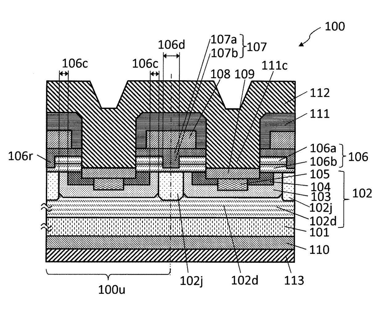
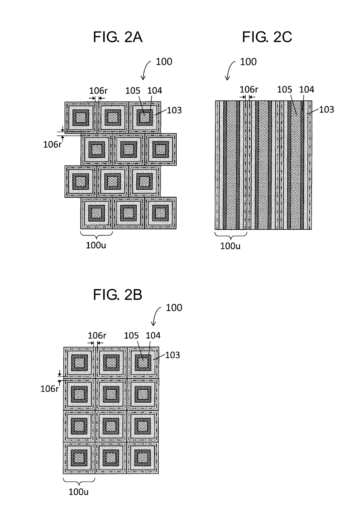
[0049]FIG. 1 schematically illustrates a cross-section of silicon carbide semiconductor element 100 according to a first exemplary embodiment. FIG. 1 is a schematic cross-sectional view of a vertical SiC-MOSFET in which two unit cells 100u are arranged side by side. Commercially available silicon carbide semiconductor element 100 includes a plurality of unit cells.

[0050](Configuration of Silicon Carbide Semiconductor Element 100)

[0051]Silicon carbide semiconductor element 100 includes semiconductor substrate 101 of a first conductivity type and first silicon carbide semiconductor layer (silicon carbide epitaxial layer) 102 of the first conductivity type located on a front surface of semiconductor substrate 101. In the present exemplary embodiment, the first conductivity type is an n type, and a second conductivity type is a p type. Howeve...

second exemplary embodiment

[0113]FIG. 8A schematically illustrates a cross-section of silicon carbide semiconductor element 200 according to the second exemplary embodiment. Silicon carbide semiconductor element 200 includes a plurality of unit cells 200u. In the present second exemplary embodiment, channel removed region106r is set to be deeper than the first exemplary embodiment. Specifically, while channel removed region 106r in the first exemplary embodiment is a cutout of second silicon carbide semiconductor layer 106, channel removed region 106r in the present second exemplary embodiment includes not only the cutout of second silicon carbide semiconductor layer 106 but also a cutout of JFET region 102j. The cutout of JFET region 102j is extended from the upper surface of JFET region 102j, and is spatially continuous with the cutout of second silicon carbide semiconductor layer 106. Note that the processes other than the channel removing process are similar to those in the first exemplary embodiment. As ...


PUM

PropertyMeasurementUnit
widthaaaaaaaaaa
widthaaaaaaaaaa
on resistanceaaaaaaaaaa

Abstract

In the silicon carbide semiconductor element, a second silicon carbide semiconductor layer that is in contact with the surface of a first silicon carbide semiconductor layer has at least an upper layer including a dopant of a first conductivity type at a high concentration. Above a junction field effect transistor (JFET) region interposed between body regions that are disposed in the first silicon carbide semiconductor layer so as to be spaced from each other, the silicon carbide semiconductor element has a channel removed region, which is a cutout formed by removing a high concentration layer from the front surface side of the second silicon carbide semiconductor layer, the high concentration layer having a higher dopant concentration than at least the dopant concentration of the JFET region. The width of the channel removed region is smaller than that of the JFET region.

Description

BACKGROUND[0001]1. Technical Field[0002]The present disclosure relates to a semiconductor element, and more particularly to a silicon carbide semiconductor element such as a power semiconductor device used for high breakdown voltage and large current, and a method for manufacturing the silicon carbide semiconductor element.[0003]2. Description of the Related Art[0004]Silicon carbide (SiC) is a high-hardness semiconductor material having a band gap larger than that of silicon (Si), and is applied to various semiconductor devices such as a power element, an environmentally-resistant element, a high-temperature operation element, and a high-frequency element. Among these elements, application to power elements, such as a semiconductor element and a rectifier element, is gaining attention. Power elements using SiC have an advantage that they can significantly reduce power loss, compared to power elements using Si. In addition, by utilizing such properties, SiC power elements can impleme...

Claims


Application Information

Patent Timeline
Patent Type & Authority Patents(United States)
IPC IPC(8): H01L29/78H01L29/66H01L29/10H01L27/06H01L29/16H01L29/80
CPCH01L29/7803H01L27/0617H01L29/105H01L29/1608H01L29/66068H01L29/1095H01L29/80H01L29/42368H01L29/7828H01L29/0696H01L29/0878
Inventor OHOKA, ATSUSHIUCHIDA, MASAOHORIKAWA, NOBUYUKIKUSUMOTO, OSAMU
Owner PANASONIC INTELLECTUAL PROPERTY MANAGEMENT CO LTD
Why Eureka
Try Eureka