

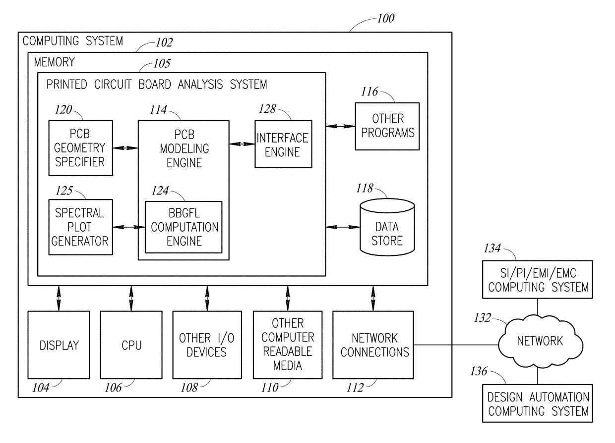
Full wave modeling and simulations of the waveguide behavior of printed circuit boards using a broadband green's function technique
a technology of green function and waveguide behavior, applied in the field of full wave modeling and simulation of waveguide behavior of printed circuit boards, can solve problems such as power integrity, electromagnetic interference, and generation of emi and emc, and achieve the effect of fast simulation
- Summary
- Abstract
- Description
- Claims
- Application Information
AI Technical Summary
Benefits of technology
Problems solved by technology
Method used
Image

Examples
example 1
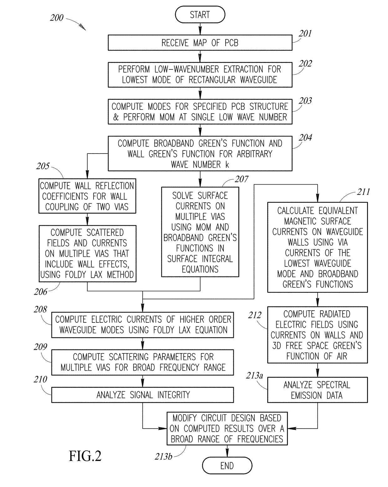
[0076]In the two-via example having a small cutout 220, L1=W1=100 mils, the two signal vias 222, 224 are located at (x,y) coordinates (−25, 0) and (25, 0) mils. FIGS. 7A-7D show plots of the S-parameters in dB over the frequency range 0-20 GHz obtained using the BBGFL / Foldy-Lax method at step 205, compared with other methods: FIG. 7A shows insertion loss; FIG. 7B shows return loss; FIG. 7C shows far end crosstalk; and FIG. 7D shows near end crosstalk. The results for all four S-parameters obtained using the BBGFL / Foldy-Lax method are in close agreement with those obtained by the MoM, MoM / Foldy-Lax approach, and the HFSS approach. All of the methods indicate the resonant frequencies (peaks), which are caused by reflections from the walls of the waveguide 214. FIGS. 8A-8D show plots of the S-parameters in dB over the frequency range 0-20 GHz obtained using the BBGFL / MoM compared with other methods. Again there is good agreement with the current methods. The results of the BBGFL theref...
example 2
[0077]The waveguide 214 has a large cutout 220 of dimension L1=200 mils×W1=100 mils. FIG. 9 shows the locations of the eight vias with respect to the waveguide 214. Four signal vias 232 are located at (−25, 50), (25, 50), (−25, −50), and (25, −50) mils; and four shorting vias 234 are located along the y-axis in pairs that are centered on the mid-points (0, −25), and (0, 25) between the signal vias 232. Results obtained using the BBGFL / Foldy-Lax approach are compared with results from other methods, in FIGS. 10A-10D. FIG. 10A shows insertion loss; FIG. 10B shows return loss; FIG. 10C shows far end crosstalk; and FIG. 10D shows near end crosstalk. Again, the results for all four S-parameters are in close agreement with those obtained by the MoM / Foldy-Lax approach, and the HFSS approach. Corresponding results obtained using the BBGFL / MoM approach are compared with results from other methods in FIGS. 11A-11D.
[0078]For the intermediate case of four vias at 1000 frequency points, the pres...
PUM
 Abstract
Description
Claims
Application Information