Light-emitting device of gallium nitride compound semiconductor

Inactive Publication Date: 2000-06-27
TOYODA GOSEI CO LTD +1
View PDF46 Cites 102 Cited by
  • Summary
  • Abstract
  • Description
  • Claims
  • Application Information

AI Technical Summary

Benefits of technology

The present invention was completed to address the above-mentioned problem. It is an object of the present invention to provide a ligh

Problems solved by technology

However, only a little has been reported on the process of producing such light-emitting diode

Method used


Image

  • Light-emitting device of gallium nitride compound semiconductor
  • Light-emitting device of gallium nitride compound semiconductor
  • Light-emitting device of gallium nitride compound semiconductor

Examples


example 1

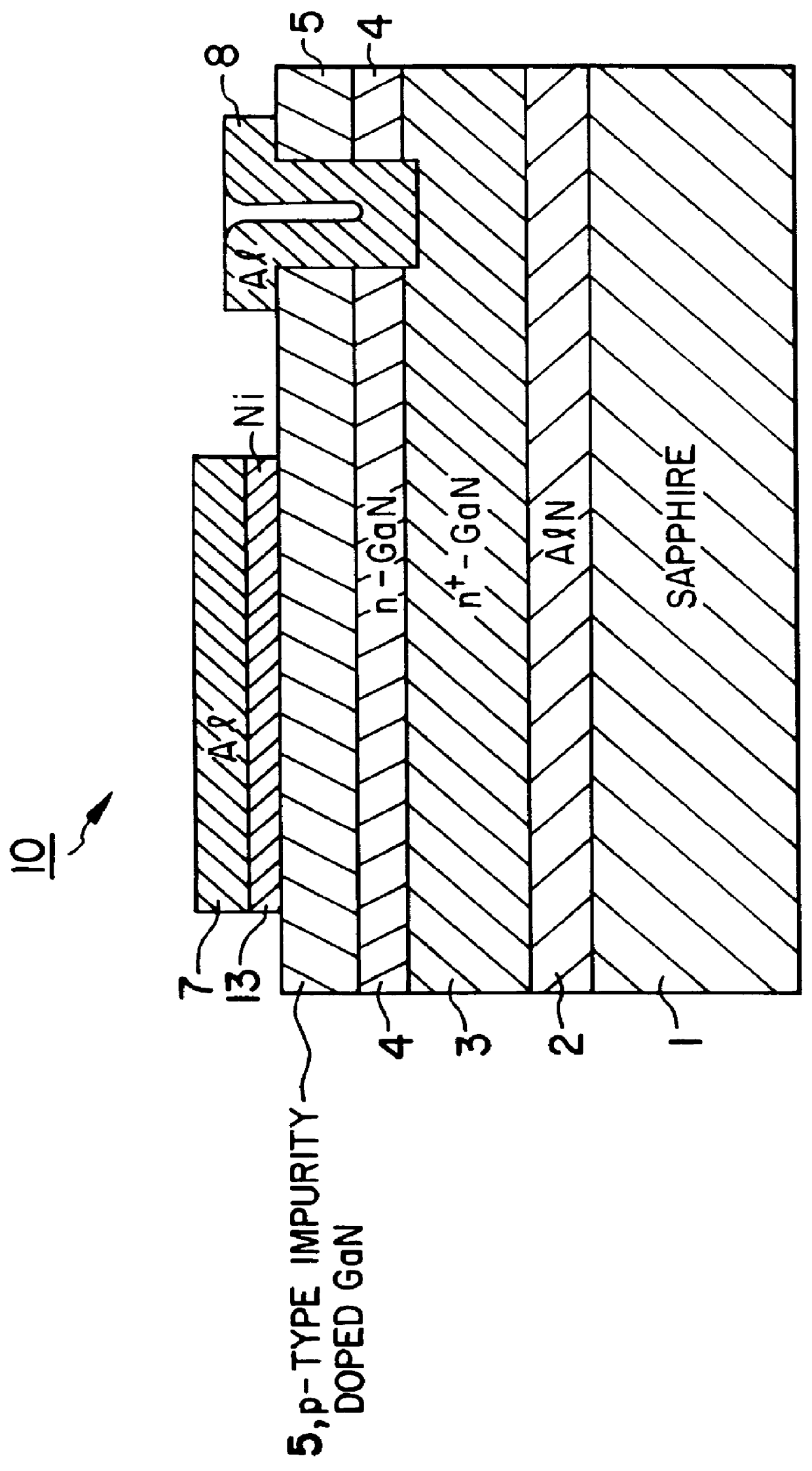
The present invention will be described in more detail with reference to a first disclosed embodiment. FIG. 1 shows a vertical section of a light-emitting diode 10 pertaining to the present invention. It has a sapphire substrate 1, on which there are successively formed a buffer layer 2 of AlN (500 .ANG. thick), a high-carrier density n.sup.+ -layer 3 of GaN (2.2 .mu.m thick), a low-carrier density n-layer 4 of GaN (1.5 .mu.m thick), an .[.i-layer.]. .Iadd.a p-type impurity doped layer .Iaddend.5 of GaN (0.1 .mu.m thick), an electrode 7 of aluminum, and an electrode 8 of aluminum (in contact with the high-carrier density n.sup.+ -layer 3).

This light-emitting diode 10 is produced by the steps which are explained below with reference to FIGS. 2(A) to 4(C).

The entire process was carried out using NH.sub.3, H.sub.2 (carrier gas), trimethyl gallium Ga(CH.sub.3).sub.3 (TMG for short), trimethyl aluminum Al(CH.sub.3).sub.3 (TMA for short), silane SiH.sub.4 and diethyl zinc (DEZ for short)....

example 2

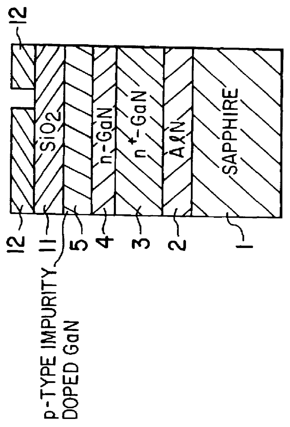
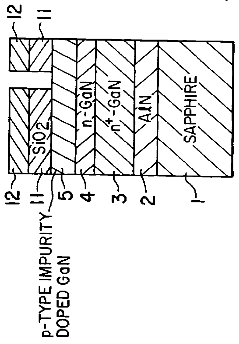
A light-emitting diode was prepared in the same manner as in Example 1. As shown in FIG. 6, it is composed of a sapphire substrate 1, a buffer layer 2 of AlN, a high-carrier density n.sup.+ -layer 3 of GaN, a low-carrier density n-layer 4 (1.1 .mu.m thick) having a carrier density of 1.times.10.sup.15 / cm.sup.3, a low-impurity density .[.i.sub.L -layer.]. .Iadd.L-layer .Iaddend.51 (1.1 .mu.m thick) having a Zn density of 2.times.10.sup.18 / cm.sup.3, and a high-impurity density .[.i.sub.H -layer.]. .Iadd.H-layer .Iaddend.52 (0.2 .mu.m thick) having a Zn density of 1.times.10.sup.20 / cm.sup.3. It should be noted that the .[.i-layer.]. .Iadd.p-impurity doped layer .Iaddend.is of dual structure with 51 and 52.

A hole 60 was formed which penetrates the high-impurity density .[.i.sub.H layer.]. .Iadd.H-layer .Iaddend.52, the low-impurity density .[.i.sub.L layer.]. .Iadd.L-layer .Iaddend.51, and the low-carrier density n-layer 4, reaching the high-carrier density n.sup.+ -layer 3. In this ...

example 3

The light-emitting diode in this example differs from that in the previous example in that the first Ni layer 71 (81) and second Ni layer 72 (82) are replaced by a Ni layer 710 (810) of single-layer structure, which is 300 .ANG. thick, as shown in FIG. 7. This difference in structure has nothing to do with its performance. The Ni layer 710 (810) should preferably have a thickness in the range of 50 .ANG. to 3000 .ANG.. With a thickness lower than specified, it will be subject to attack by solder when a solder bump is formed. With a thickness greater than specified, it causes the light source to be localized near the electrode rather than the center and it is liable to peeling at the time of soldering in a solder bath.


PUM


Abstract

A light-emitting diode of GaN compound semiconductor emits a blue light from a plane rather than dots for improved luminous intensity. This diode includes a first electrode associated with a high-carrier density n+ layer and a second electrode associated with a high-impurity density [iH-layer] H-layer. These electrodes are made up of a first Ni layer (110 ANGSTROM thick), a second Ni layer (1000 ANGSTROM thick), an Al layer (1500 ANGSTROM thick), a Ti layer (1000 ANGSTROM thick), and a third Ni layer (2500 ANGSTROM thick). The Ni layers of dual structure permit a buffer layer to be formed between them. This buffer layer prevents the Ni layer from peeling. The direct contact of the Ni layer with GaN lowers a drive voltage for light emission and increases luminous intensity.

Description

BACKGROUND OF THE INVENTION1. Field of the InventionThe present invention relates to a light-emitting device of gallium nitride compound semiconductor which emits a blue light.2. Description of the Prior ArtAmong the conventional light-emitting diodes which emit a blue light is the gallium nitride compound semiconductor. It attracts attention because of its high luminous efficiency resulting from the direct transition and its ability to emit a blue light, one of the three primary colors of light.The light-emitting diode of gallium nitride compound semiconductor is made up of a sapphire substrate, an n-layer grown on the substrate from a GaN compound semiconductor of n-type conduction, with or without a buffer layer of aluminum nitride interposed between them, and .[.an i-layer.]. .Iadd.a p-type impurity doped layer .Iaddend.grown on the n-layer from a GaN compound semiconductor which is made .[.i-type.]. by doping with a p-type impurity. (Japanese Patent Laid-open Nos. 119196 / 1987 a...

Claims


Application Information

Patent Timeline
IPC IPC(8): H01L33/00H01L33/32H01L33/38H01L33/40
CPCH01L33/0037H01L33/40H01L33/38H01L33/32H01L33/382
Inventor MANABE, KATSUHIDEKOTAKI, MASAHIROTAMAKI, MAKOTOHASHIMOTO, MASAFUMI
Owner TOYODA GOSEI CO LTD
Why Eureka
Try Eureka