
Digital analog converter and electronic device using the same

A converter circuit, display device technology, applied in the direction of digital-to-analog converter, analog/digital conversion, code conversion, etc.

Inactive Publication Date: 2008-10-01
SEMICON ENERGY LAB CO LTD
View PDF11 Cites 1 Cited by
  • Summary
  • Abstract
  • Description
  • Claims
  • Application Information

AI Technical Summary

Problems solved by technology

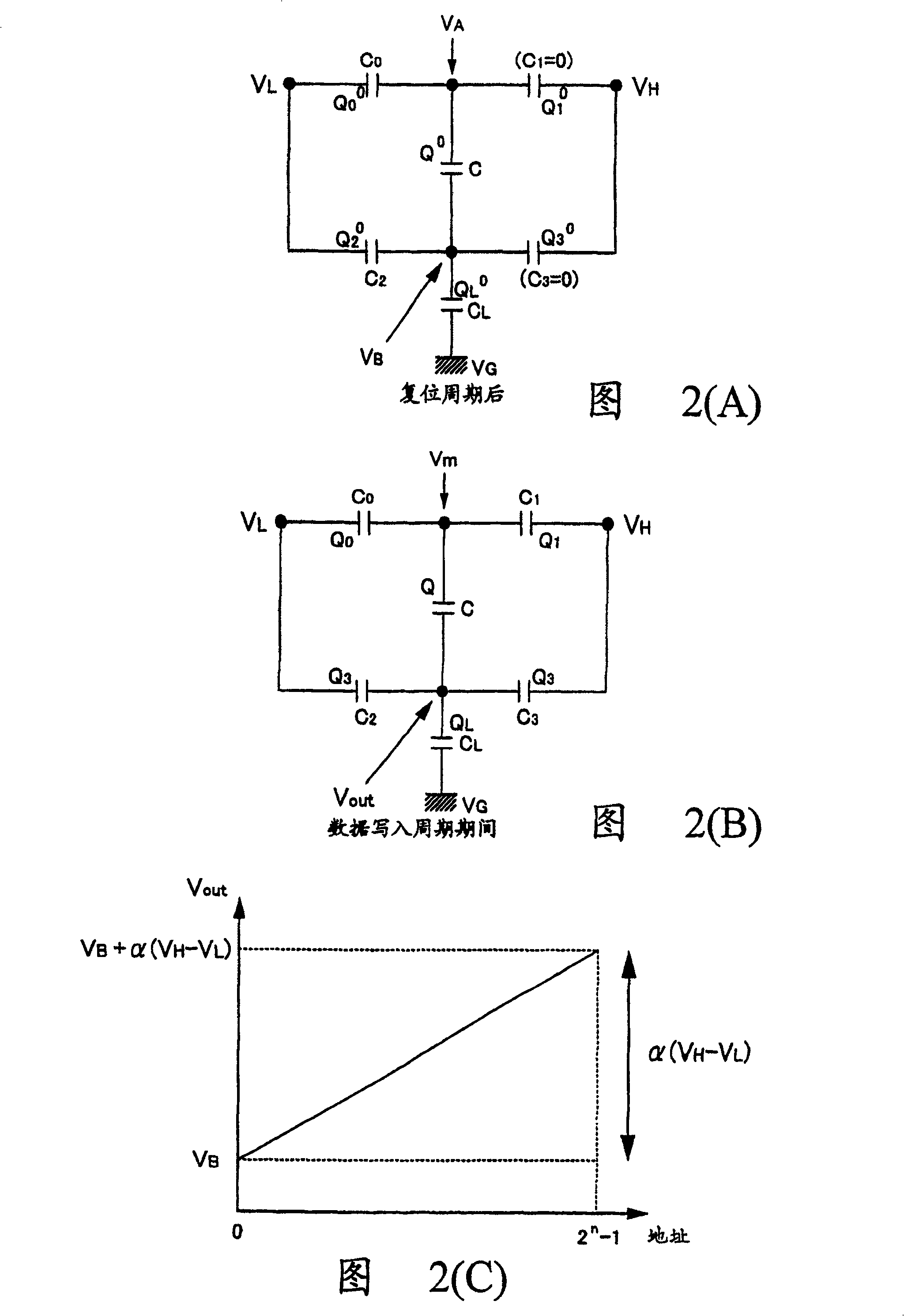
But since according to expressions (26) and (27), the output V out depends on V H and V L difference, and varies with respect to the address of the digital data with respect to the V L varies in a linear fashion, it is not possible to independently control the output V out The voltage amplitude and reference potential of

Method used


Image

  • Digital analog converter and electronic device using the same
  • Digital analog converter and electronic device using the same
  • Digital analog converter and electronic device using the same

Examples


Embodiment 1

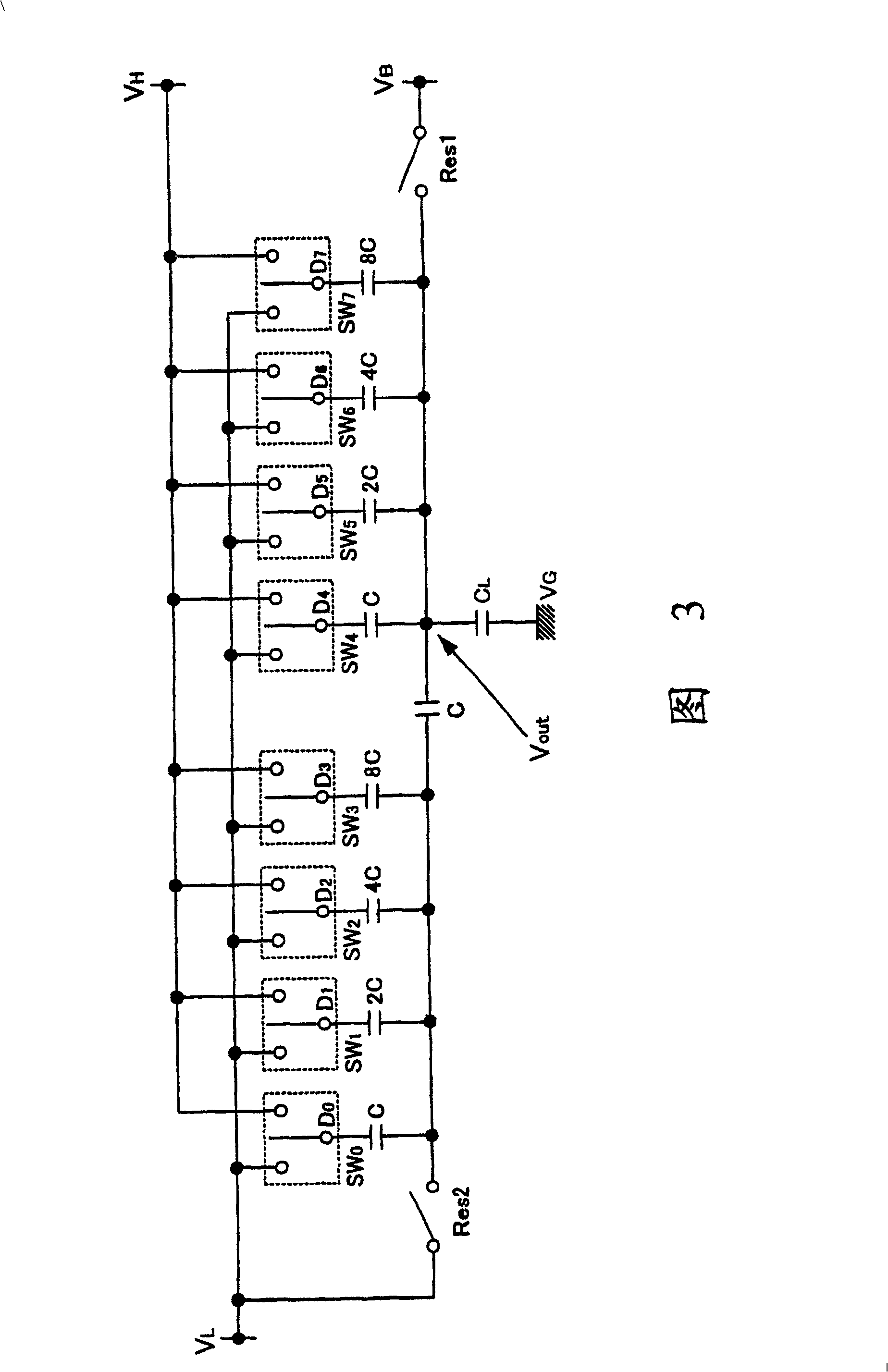
[0134] Fig. 3 shows a circuit diagram of the 8-bit DAC of the embodiment.

[0135] Figure 3 shows an embodiment where the DAC is managed by 8 bits (D 0 (LSB) to D 7 (MSB)) digital data. Also, 8-bit digital data is divided into lower 4 bits (D 0 to D 3 ) and upper 4 bits (D 4 to D 7 ).

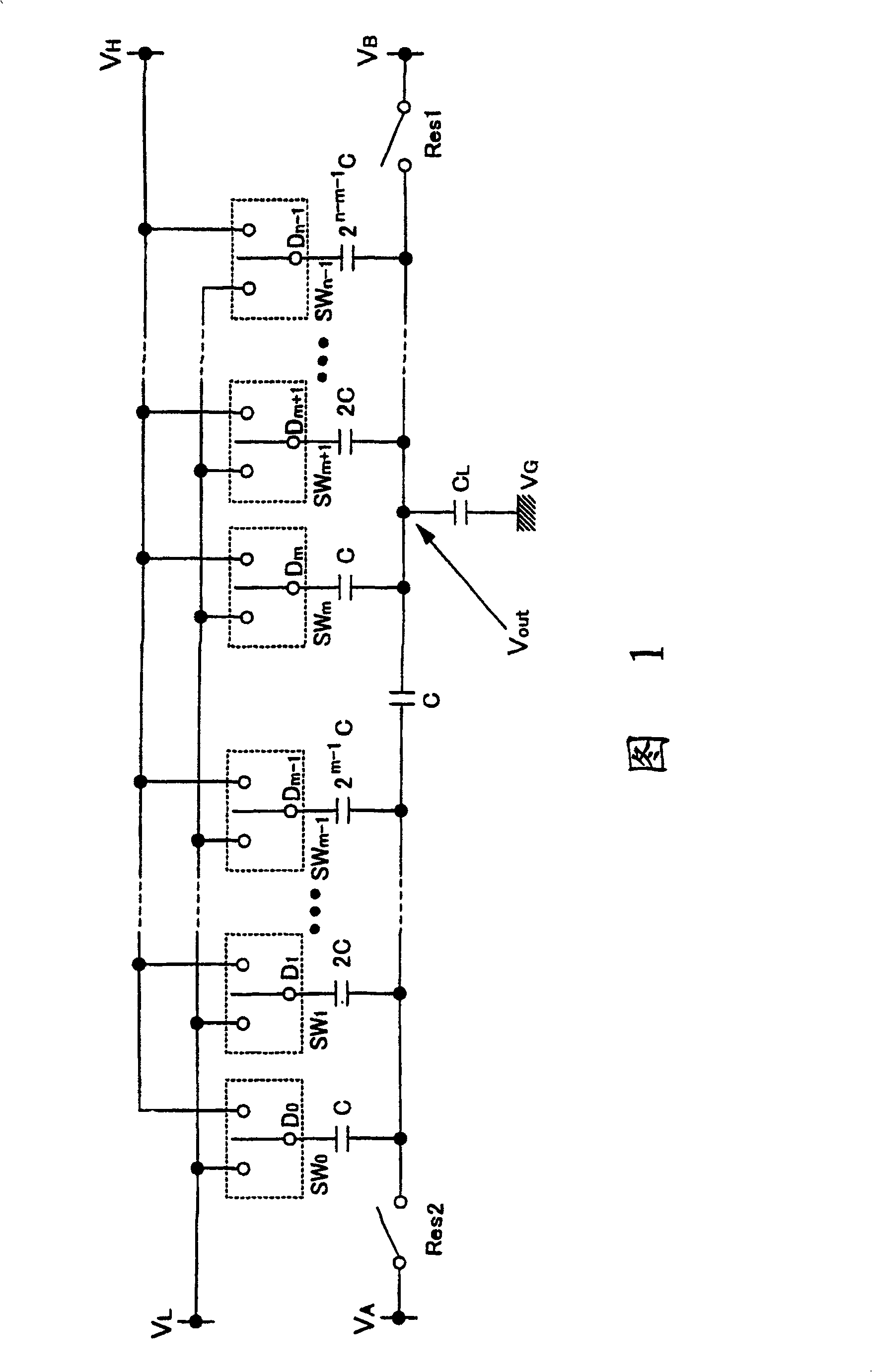
[0136] The DAC of this embodiment shown in Figure 3 has each bit (D 0 to D 7 ), connected to each switch (SW 0 to SW 7 ) capacitors (C, 2C, 4C, 8C, C, 2C, 4C, and 8C) and eight switches (SW 0 to SW 7 ). Also, the DAC of the present embodiment has a capacitor that connects the circuit portion corresponding to the lower 4 bits to the circuit portion corresponding to the upper 4 bits.

[0137] Power V H and V L and offset supply V B is connected to a DAC according to the invention.

[0138] Switch (SW 0 to SW 7 ) in each bit of input digital data (D 0 to D 7 ) is 0(L O ) is connected to the power supply V L , while each bit of the input digital data (D 0 to D 7 ) is connec...

Embodiment 2

[0179] In this embodiment, a case where the DAC according to Embodiment 1 above is used for a driving circuit of an active matrix type liquid crystal display device will be described.

[0180] Figure 5 is a general block diagram of the active matrix type liquid crystal display device according to the present embodiment, in which the source signal line driving circuit A is represented by 501, the source signal line driving circuit B is represented by 502, and the gate signal line driving circuit is represented by 503 , an active matrix circuit is represented by 504 , and a digital video data dividing circuit (SPC: Serial Parallel Conversion Circuit) is represented by 505 .

[0181] The source signal line drive circuit A 501 has a shift resistor circuit (240 stages×2 shift register circuits) 501-1, a latch circuit 1 (960×8 digital latch circuits) 501-2, a latch circuit Circuit 2 (960×8 digital latch circuit) 501-3, selector circuit 1 (240 selector circuit) 501-4, D / A converter ...

Embodiment 3

[0262] In Embodiment 3, another method for producing an active matrix type liquid crystal display device having a DAC according to the present invention, which is different from the production method described in Embodiment 2 above, is given. Also, the active matrix type liquid crystal display device according to this embodiment can be used as the active matrix type liquid crystal display device of Embodiment 2.

[0263] Take Figure 16(A) as a reference. First, an underlayer composed of a silicon oxide layer 5002 is formed on a glass substrate 5001 to a thickness of 200 nm. The bottom layer may be obtained by superposing a silicon nitride layer or may consist only of a silicon nitride layer.

[0264] Next, an amorphous silicon layer 4003 was formed to a thickness of 30 nm by using the plasma CVD method on the silicon oxide layer 5002, and then dehydrogenated. Thereafter, a polysilicon layer (crystallized silicon layer or polysilicon layer) is deactivated by an excimer laser ...


PUM

PropertyMeasurementUnit
lengthaaaaaaaaaa
thicknessaaaaaaaaaa
thicknessaaaaaaaaaa

Abstract

The present invention relates to a D / A converter circuit capable of independently controlling the output voltage amplitude V out and reference voltage. The D / A converter circuit converts "n"-bit digital data ("n": natural number) into an analog signal, where each bit of the "n"-bit digital data controls a switch, which controls the charge in a capacitor connected to the switch charging and discharging, and output an analog signal with an offset potential used as a reference potential.

Description

[0001] This application is a divisional application of the application dated December 3, 1999, the application number is 99127871.2, and the invention title is a digital-to-analog converter and electronic equipment using it. technical field [0002] The present invention relates to a D / A converter (digital / analog converter) circuit (DAC), and more particularly to a DAC for a driver circuit of an active matrix type semiconductor device. Also, the present invention relates to an active matrix type semiconductor display device using such a DAC. Background technique [0003] Recently, technologies for producing semiconductor devices such as thin film transistors (TFTs) having semiconductor thin films formed on inexpensive glass substrates have been rapidly developed. The reason is increasing demand in active matrix type liquid crystal display devices. [0004] Active matrix liquid crystal display devices are such that pixel TFTs are arranged on a pixel area composed of tens of ...

Claims


Application Information

Patent Timeline
Patent Type & Authority Patents(China)
IPC IPC(8): G09G3/36G09G3/20H03M1/66G02F1/133G09G3/32H03M1/68H03M1/74H03M1/80
CPCG09G3/3233G09G3/3275G09G3/3648G09G3/3688G09G2300/0417G09G2300/0426G09G2300/0842G09G2310/027G09G2310/0297G09G2330/02H03M1/0607H03M1/68H03M1/804H03M1/66
Inventor 浅见宗广纳光明盐野入丰长尾祥
Owner SEMICON ENERGY LAB CO LTD
Learn More