Supercharge Your Innovation With Domain-Expert AI Agents!

Gate electrode and manufacturing method thereof

A manufacturing method and gate electrode technology, applied in semiconductor/solid-state device manufacturing, circuits, electrical components, etc., can solve problems such as difficult to mature technology, opening is difficult to use in opening size, and cannot be mass-produced

Inactive Publication Date: 2008-11-19
FUJITSU LTD
View PDF8 Cites 0 Cited by
  • Summary
  • Abstract
  • Description
  • Claims
  • Application Information

AI Technical Summary

Problems solved by technology

That is, in the case of (1) above, although the diameter of the electron beam can be miniaturized to about 0.04 μm by using the existing technology, it is difficult to say that it is very mature when considering the manufacturing stability when integrating thousands of transistors, etc. Technology
In addition, in the case of (2) above, the amount of reduction in the opening size obtained stably is within 0.04 μm, and a large reduction in the opening size exceeding this value still has problems in uniformity and cannot be used for mass production.
In addition, it is difficult to use the same opening for the opening for forming the groove and the opening for forming the gate electrode, which have a large difference in opening size.

Method used


Image

  • Gate electrode and manufacturing method thereof
  • Gate electrode and manufacturing method thereof
  • Gate electrode and manufacturing method thereof

Examples


Embodiment 1

[0164] On a semi-insulating GaAs substrate, a buffer layer, an InGaAs electron transport layer, an AlGaAs electron supply layer, and a GaAs low-resistance layer are sequentially stacked by MOCVD. In addition, after forming an active region by implanting oxygen, AuGe (20nm ) / Au(200nm) electrode to form an ohmic electrode.

[0165] Next, in the aforementioned active region in the gate electrode formation region, at both ends of the portion where the fine grid (gate electrode) is to be formed, the low-resistance layer portion in the region with a width of about 0.2 μm is excavated and removed to form a groove region. .

[0166] Secondly, if figure 2 As shown, on the substrate 1 on which the gate electrode is formed, a PMMA-based protective film (ZEP2000, manufactured by Japan Zeon (company name) Co., Ltd.) is coated with a thickness of 300 nm by spin coating, and heat-treated at 180° C. for 5 minutes. This forms the lowermost layer 2 . PMGI (manufactured by MCC Co., Ltd.) was...

Embodiment 2

[0175] Example 1 is the same as Example 1, except that the gate electrode forming surface driving step is performed after the gate electrode opening forming step and before the electron beam incident step and the gate electrode opening narrowing step.

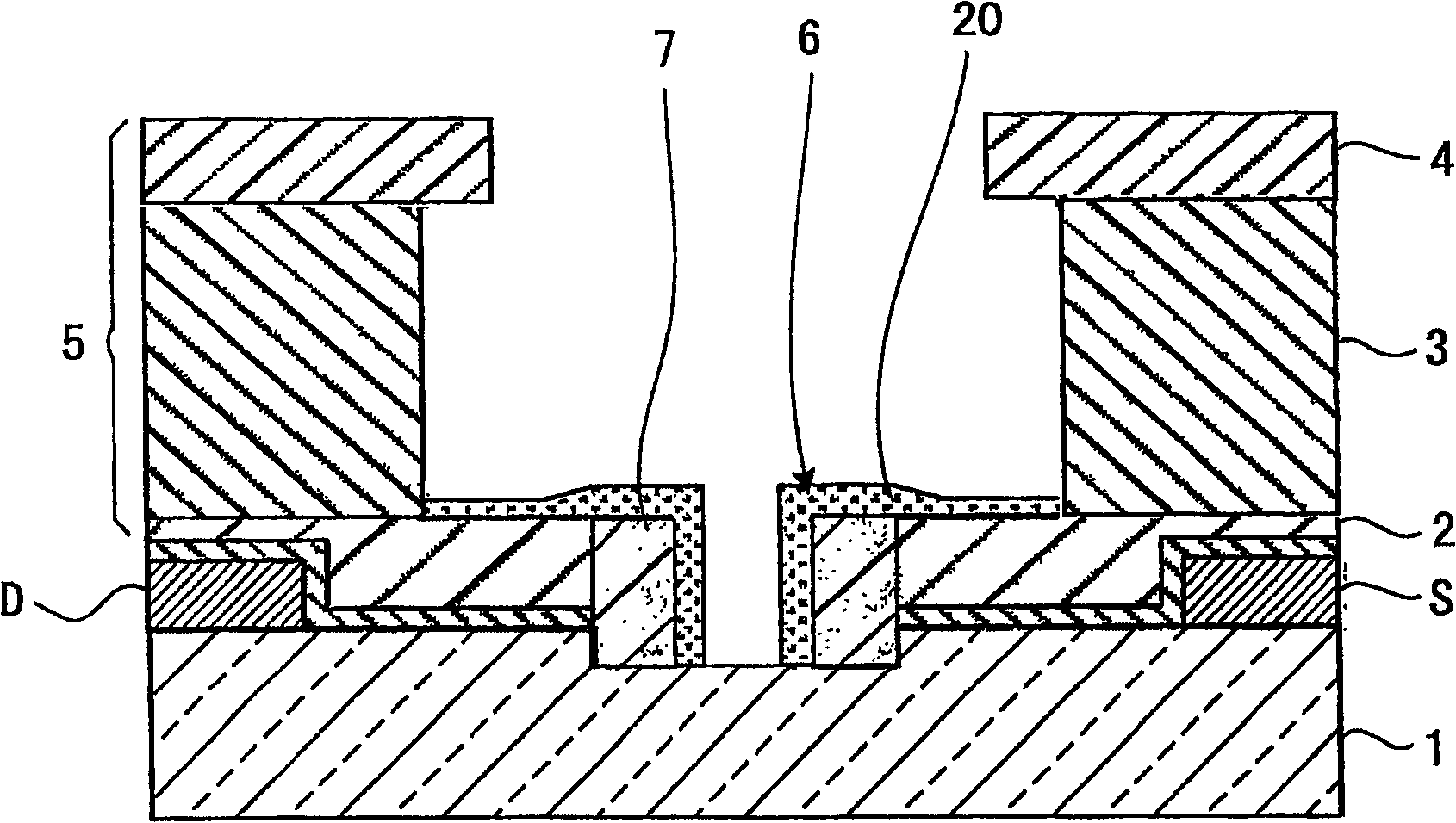
[0176] That is, specifically, as Figure 4A As shown, on the surface of the semiconductor substrate, source electrodes S and drain electrodes D are formed at regular intervals, and a SiN film is formed. Then, a multilayer protective layer 5 composed of the lowermost layer 2 , the intermediate layer 3 and the uppermost layer 4 is formed on the SiN film through the aforementioned multilayer protective layer forming step. Next, openings are formed in the uppermost layer 4 and the intermediate layer 3 in the laminated protective layer 5 through the aforementioned opening forming step. Then, the opening 10 for the gate electrode having an opening size of 0.2 μm was formed by the aforementioned opening forming step for the gate elec...

Embodiment 3

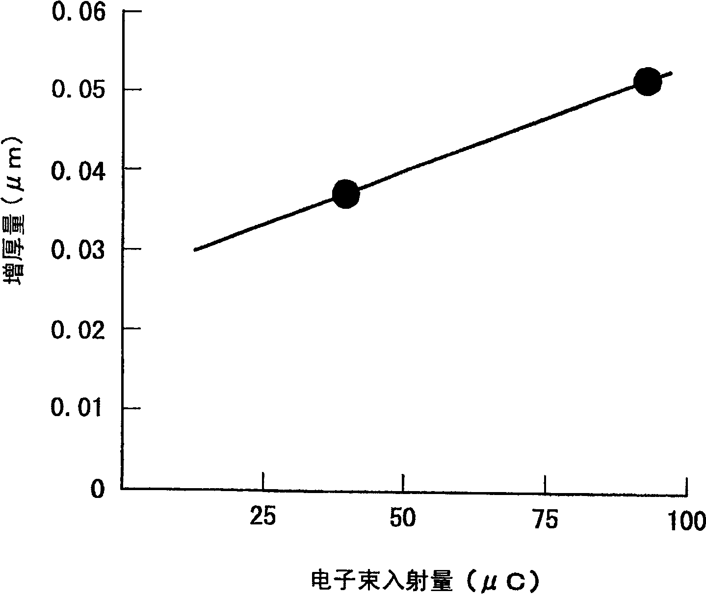
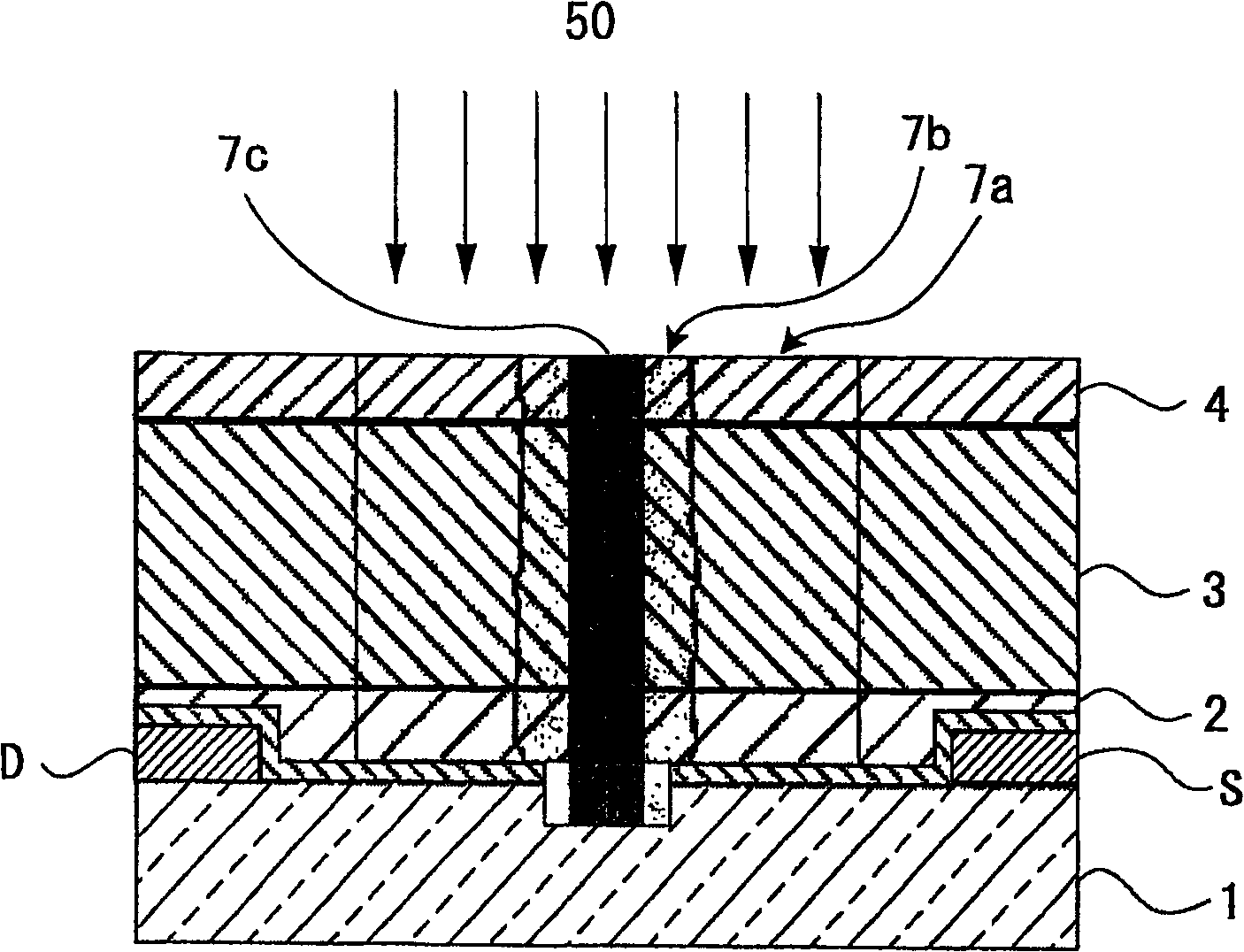
[0182]In Example 2, in the aforementioned electron beam incident step, since the opening size of the drain electrode D side of the gate electrode opening is selectively reduced, the incident is insufficient to develop Eth only on the drain electrode D side. Dose (60μC) (reference Figure 5A ~C).

[0183] results, such as Figure 5D As shown, for the gate electrode 30, the groove length on the D side of the drain electrode is 0.04 μm longer than the groove length on the S side of the source electrode, resulting in a field effect transistor with an offset gate.

[0184] Here, if the preferred mode of the present invention is annotated, it is as follows:

[0185] (Supplementary Note 1) A method for manufacturing a gate electrode, characterized by comprising: a step of forming a laminated protective film including an electron beam protective layer at least in the lowermost layer on a gate electrode forming surface; An opening forming step of forming an opening in a layer other ...


PUM


Abstract

A method for fabricating a micro gate electrode by reducing the dimensions of an opening formed by a conventional electron beam lithography by increasing the thickness of the opening. The method comprises a multilayer resist forming step of forming a multilayer resist including an electron beam resist layer as a lowermost layer on a gate electrode forming surface, an opening forming step of forming an opening extending through the other layers than the lower most layer, a gate electrode opening forming step of forming an opening for a gate electrode in the lowermost layer, a gate electrode opening reducing step of selectively reducing the opening for the gate electrode, and a gate electrode forming step of forming the gate electrode in the opening for the gate electrode. The gate electrode opening reducing step of a preferable mode is such that a material for increasing the thickness of a resist pattern is applied to the surface of the lowermost layer at least once to reduce the dimensions of the opening for the gate electrode. Another preferable mode includes an electron beam directing step of directing an electron beam to the vicinity of the opening for the gate electrode before the gate electrode opening reducing step.

Description

technical field [0001] The present invention relates to a method for manufacturing a gate electrode, a gate electrode manufactured by the method for manufacturing the gate electrode, a semiconductor device using the gate electrode, and a method for manufacturing the same. The formed gate electrode is thickened with a protective film opening to reduce the opening size, and a fine gate electrode can be manufactured efficiently. This gate electrode has excellent high-frequency characteristics and is suitable for transmission and reception of submillimeter and millimeter wave bands and high-speed signal processing. A field-effect transistor useful as a (optical communication) device. Background technique [0002] A field-effect transistor excellent in high-frequency characteristics is useful as a device for transmitting and receiving radio waves in the submillimeter and millimeter wave bands, and as a device for high-speed signal processing (for optical communication). Among th...

Claims


Application Information

Patent Timeline
Patent Type & Authority Patents(China)
IPC IPC(8): H01L29/80H01L21/28H01L21/027G03F7/40H01L21/338H01L29/423H01L29/812
CPCH01L21/28H01L21/0272H01L29/42316
Inventor 牧山刚三野崎耕司
Owner FUJITSU LTD
Features
  • R&D
  • Intellectual Property
  • Life Sciences
  • Materials
  • Tech Scout
  • Unparalleled Data Quality
  • Higher Quality Content
  • 60% Fewer Hallucinations
Learn More