Two-frequency wideband electromagnetic band gap structure and making method

An electromagnetic bandgap structure, broadband technology, applied in the direction of radiation element structure, circuits, electrical components, etc., to shorten the patch geometry, reduce mutual coupling, and suppress surface waves.

Inactive Publication Date: 2008-12-03
SHANGHAI INST OF MICROSYSTEM & INFORMATION TECH CHINESE ACAD OF SCI
View PDF7 Cites 2 Cited by
  • Summary
  • Abstract
  • Description
  • Claims
  • Application Information

AI Technical Summary

Problems solved by technology

However, with the miniaturization of communication equipment today, the size of microwave devices and antennas in the centimeter band is required to be more and more miniaturized and integrated. Materials with relatively low dielectric constants such as silicon often cannot meet this miniaturization requirement. Therefore, the preparation of high dielectric constant electromagnetic bandgap structures and their applications has become the goal of everyone's expectations.

Method used


Image

  • Two-frequency wideband electromagnetic band gap structure and making method
  • Two-frequency wideband electromagnetic band gap structure and making method
  • Two-frequency wideband electromagnetic band gap structure and making method

Examples


Embodiment Construction

[0032] The substantive features and remarkable progress of the present invention are further clarified through the following specific embodiments.

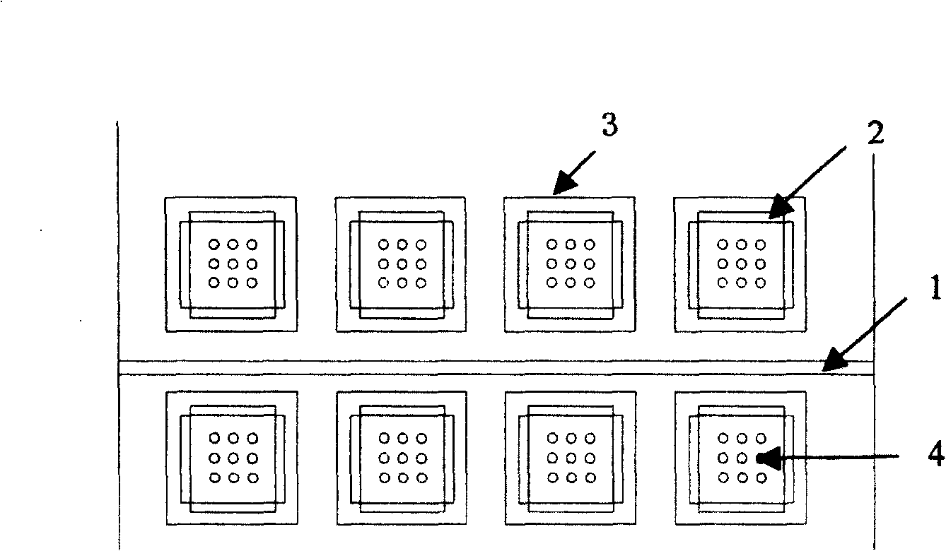
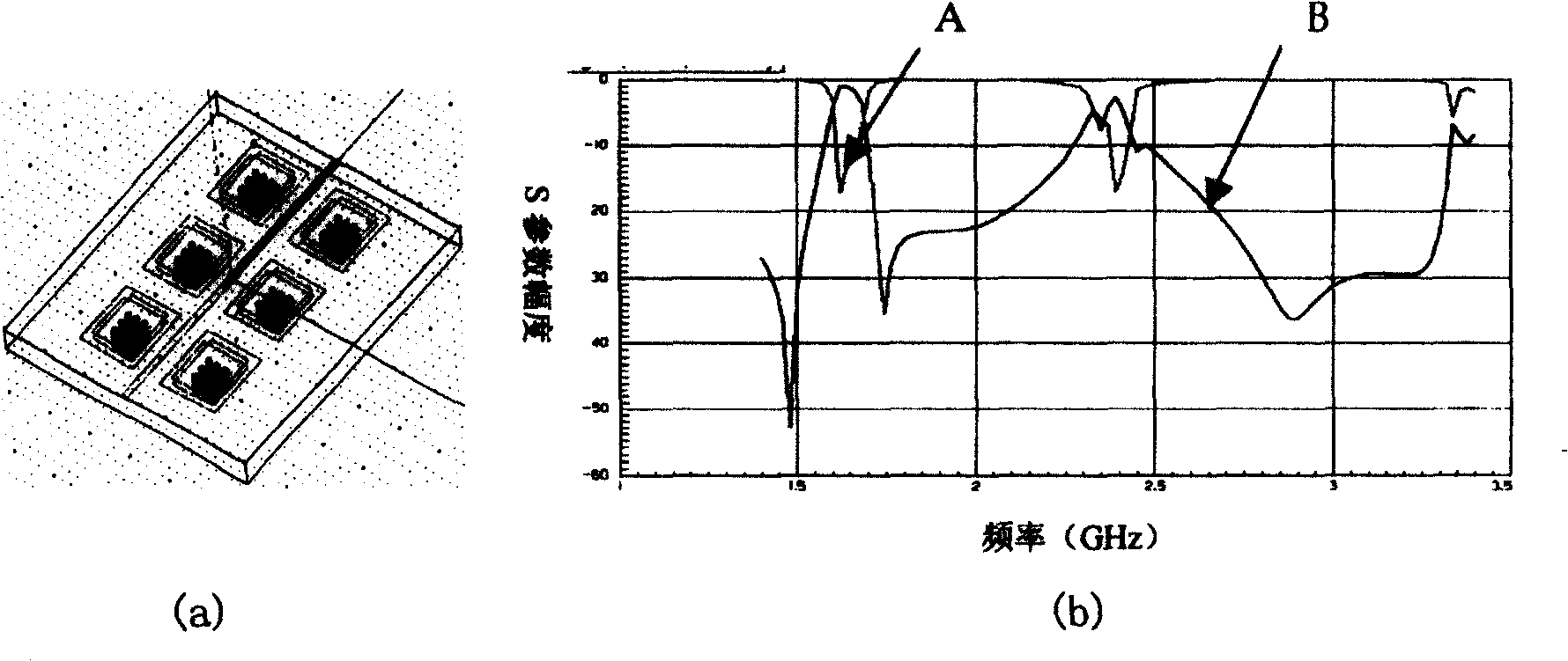
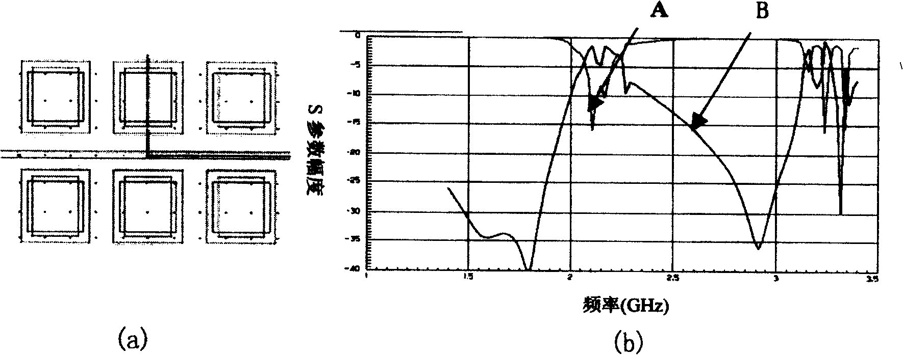
[0033] In order to shorten the size of the structural unit, the ε r =20 high dielectric constant (referred to as high K material) microwave dielectric material as the substrate, designed a dual-frequency broadband perforated high-resistance surface structure (see attached figure 1 ). Depend on figure 1 It can be seen that the dielectric substrate is rectangular (80mm×60mm×3mm); the surface of the dielectric is closely attached to a high-resistance surface electromagnetic bandgap (EBG) structure, which consists of three parts: a periodic metal patch unit (square, size 13.8mm×13.8mm), perforated narrow gaps on the patch unit (a total of 4 on each patch, with a size of 9mm×1mm) and metal cylinders with a distance of 2mm on the patch unit (a total of 4 on each patch) 9, the height is 3mm, the diameter is Φ=1mm), etc.; there is a 50...


PUM


Abstract

This invention provides a double frequency wide band electromagnetic band gap (EBG) structure and its manufacturing method characterizing that the provided structure is a mixed one combining a punch structure and a high resistant surface structure, the medium substrate in the EBG structure is square with the punch and high resistant structure adhered closely on its surface, the central frequencies of the stop-bands are 1.6GHZ and 2.4GHz. The punch and high resistant structures are composed of a periodical metal plate unit, punch narrow gaps and metallic post on the plate. According to a known work frequency, the medium thickness and its dielectric constant, the micro-band line width, the sizes of the substrate, the quadrant metallic plate and high resistant surface gap are computed preliminarily then to determine its final sizes by optimizing and emulating utilizing the emulation software of HFSS8.0 edition.

Description

technical field [0001] The invention relates to a novel electromagnetic bandgap (EBG) structure and a manufacturing method with dual-band band-resistance characteristics, and belongs to the technical field of electromagnetic wave propagation and reception. Background technique [0002] As we all know, in the modern society with the rapid development of science and technology, the emergence of semiconductors has brought a profound impact on our life and the development of science and technology. The functions of almost all semiconductor devices are realized by utilizing and controlling the movement of electrons. However, due to the limitation of the characteristics of the electron itself, the integration of semiconductor devices has reached the limit state. Photons have superior characteristics that electrons do not have: fast transmission speed and no interaction. Therefore, people hope to obtain new materials, which can freely control photons just like controlling electro...

Claims


Application Information

Patent Timeline
Patent Type & Authority Patents(China)
IPC IPC(8): H01P1/20H01Q1/38
CPCH01P1/2005
Inventor 孙晓玮包乌云包秀龙
Owner SHANGHAI INST OF MICROSYSTEM & INFORMATION TECH CHINESE ACAD OF SCI
Why Eureka
Try Eureka