Method for analyzing BEOL testing chip on-line failure

A failure analysis and chip technology, applied in electronic circuit testing, single semiconductor device testing, semiconductor/solid-state device testing/measurement, etc., can solve the problems of time-consuming and labor-intensive success rate, inability to optimize, low success rate, etc., to improve analysis efficiency and success rate, improve efficiency and accuracy, avoid the effect of destructive analysis

Inactive Publication Date: 2008-12-10
SHANGHAI HUAHONG GRACE SEMICON MFG CORP
View PDF3 Cites 0 Cited by
  • Summary
  • Abstract
  • Description
  • Claims
  • Application Information

AI Technical Summary

Problems solved by technology

Moreover, in order to ensure a certain capture rate for commonly used test structures such as open and short (Open&Short), the size of the test structure is generally above 1000 microns. It will be very time-consuming and laborious to search manually and the success rate is very low.
[0003] With the failure analysis method of the test chip in the above prior art, although its final test result can reflect the capture rate of each detection layer, it cannot pass point-to-point for the undetected defects found in failure analysis (failure analysis, hereinafter referred to as FA). program adjustments to optimize
[0004] The existing back end of line (BEOL) test chip online failure analysis method of the existing chip production line has the characteristics of strong destructiveness, low efficiency, and low success rate, and it cannot target the unidentified problems discovered by FA. Detected defects are adjusted and optimized, and there are shortcomings such as insufficient feedback for detection program optimization

Method used


Image

  • Method for analyzing BEOL testing chip on-line failure
  • Method for analyzing BEOL testing chip on-line failure

Examples


Embodiment Construction

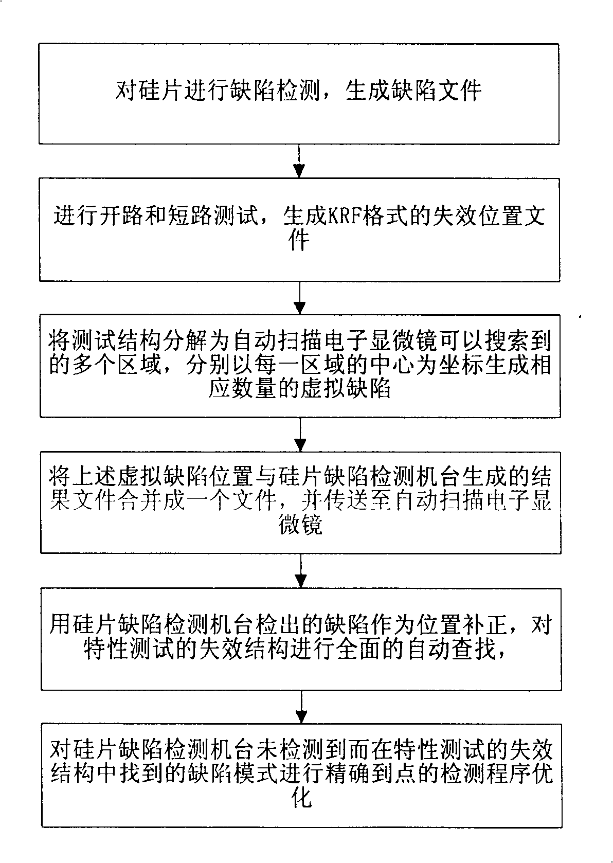
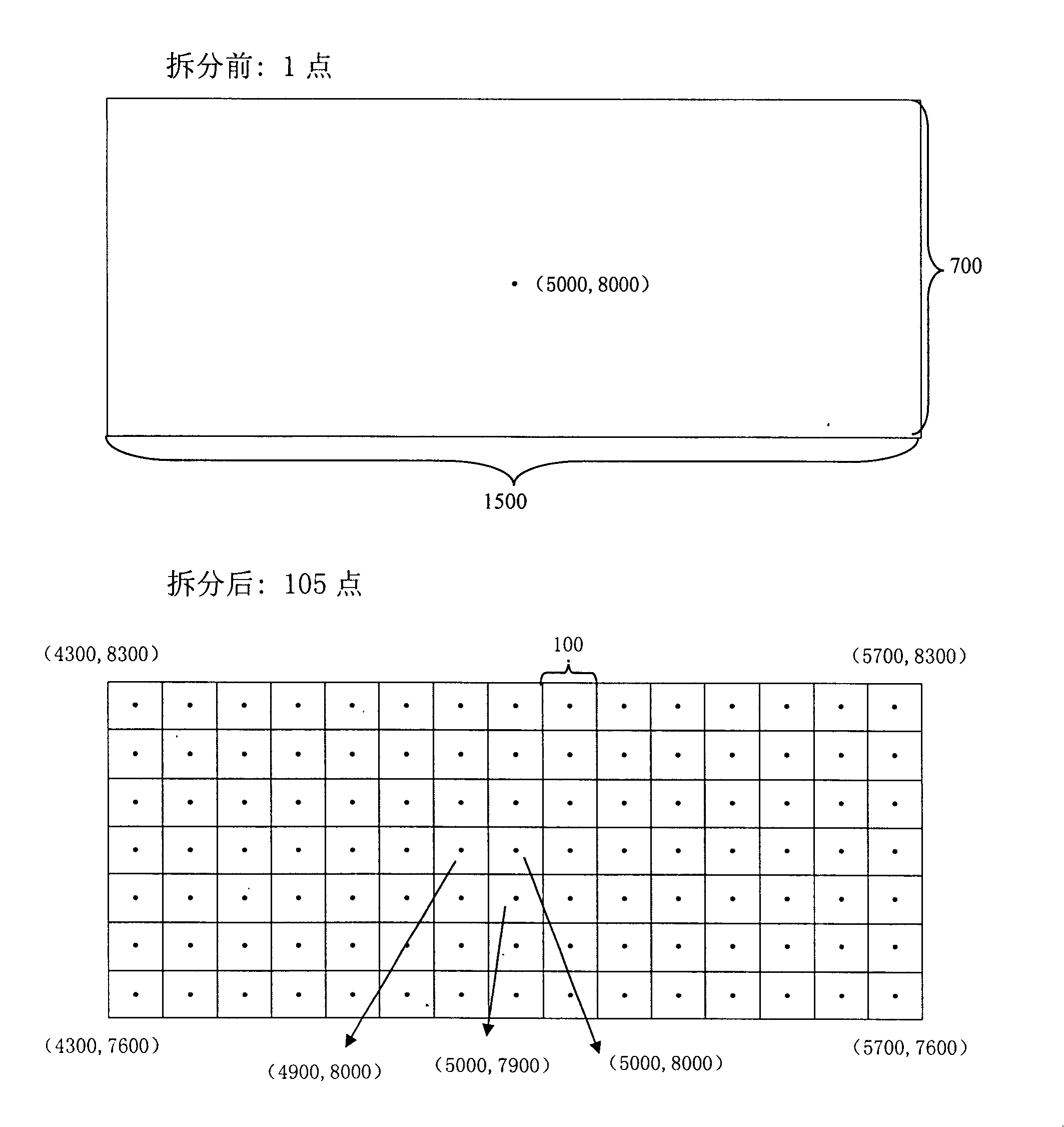
[0011] figure 1 It is a schematic flow chart of the present invention. Such as figure 1 As shown, firstly, the silicon wafer defect inspection machine is used for any layer of metal line engineering to detect the defects of the silicon wafer, and classify the detected defects, and select 5-10 point scanning electron microscopes at different positions of the silicon wafer Download the defects that are easy to find and whose size is less than 5 microns, and generate the KRF format result file ins.krf; then use the characteristic tester to perform open circuit and short circuit tests on the silicon chip, and also generate the KRF format failure location file pcm.krf, in In the above process, it is necessary to ensure that the origin of the silicon wafer and the origin of the chip of ins.krf and pcm.krf are consistent; figure 2 Schematic representation of multiple virtual defects generated for a failure structure for split feature testing. Such as figure 2 As shown, each fai...


PUM


Abstract

The invention discloses a method for online failure analysis of a BEOL test chip. The invention generates a plurality of virtual defects by splitting the failure structure of the characteristic test, and synthesizes the detection result of the defect, so as to realize the search, confirmation and analysis of the failure position by the automatic automatic scanning electron microscope. The invention can avoid the destructive analysis of the silicon chip, improve the analysis efficiency and success rate, realize the real-time feedback to the detection program at the same time, and improve the efficiency and accuracy of the program optimization. The invention is suitable for the online failure analysis method of the BEOL test chip in the semiconductor process.

Description

technical field [0001] The invention relates to a semiconductor manufacturing process, in particular to a method for online failure analysis of a BEOL test chip in the semiconductor process. Background technique [0002] The failure analysis of the test chip plays a very important role in the semiconductor process, and is generally performed after the last layer of metal lines is completed. The methods used are mainly De-Layer by chemicals, Polishing by chemical mechanical grinding, and destructive means such as Focused Ion Beam (FIB). Moreover, in order to ensure a certain capture rate for commonly used test structures such as open and short (Open&Short), the size of the test structure is generally more than 1000 microns. It will be very time-consuming and laborious to search manually and the success rate is very low. [0003] With the failure analysis method of the test chip in the above prior art, although its final test result can reflect the capture rate of each detect...

Claims


Application Information

Patent Timeline
Patent Type & Authority Patents(China)
IPC IPC(8): G01R31/00G01R31/02G01R31/26G01R31/28H01L21/66
Inventor 殷建斐
Owner SHANGHAI HUAHONG GRACE SEMICON MFG CORP
Why Eureka
Try Eureka