Supercharge Your Innovation With Domain-Expert AI Agents!

Method for cleaning residual metal

A technology for residual metal and residue removal, which is applied in electrical components, semiconductor/solid-state device manufacturing, circuits, etc., and can solve problems such as damage

Active Publication Date: 2009-03-04
UNITED MICROELECTRONICS CORP
View PDF6 Cites 0 Cited by
  • Summary
  • Abstract
  • Description
  • Claims
  • Application Information

AI Technical Summary

Problems solved by technology

As shown in Figure 4, although the HPM removal process can effectively remove unreacted platinum, the transition metal silicide 30 formed on the substrate 12 will also interact with the chlorine gas (Cl) in the HPM removal process. 2 ) and other chemical components react, and then part of the transition metal silicide 30 is corroded and peeled off, forming a damaged region 42

Method used


Image

  • Method for cleaning residual metal
  • Method for cleaning residual metal
  • Method for cleaning residual metal

Examples


Embodiment Construction

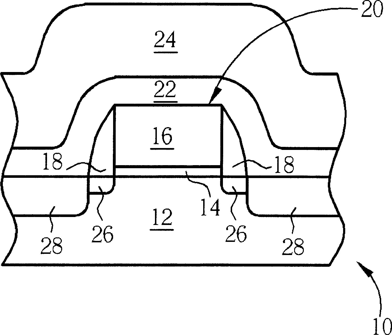
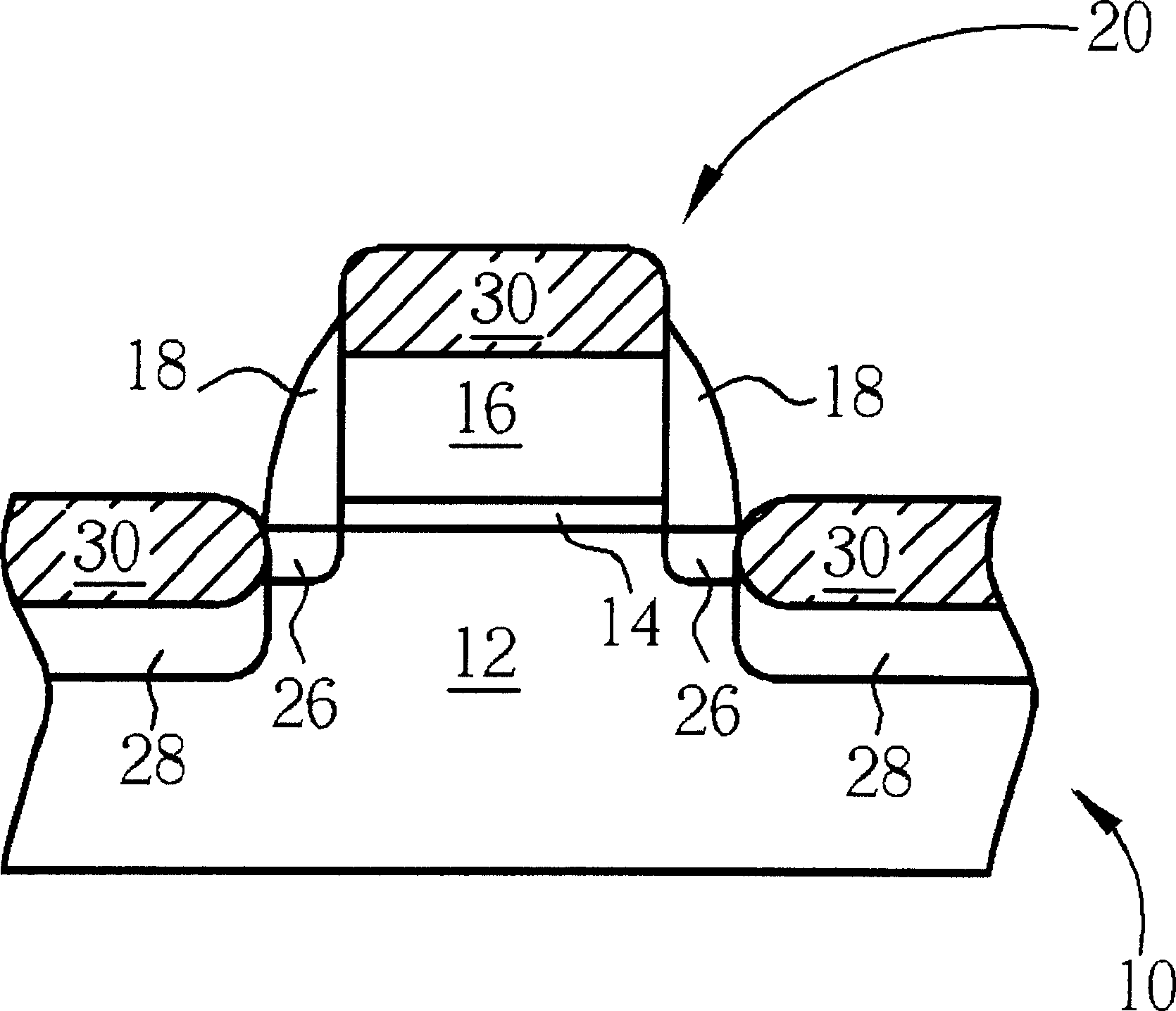
[0041] Please refer to Figures 5 to 6 , Figures 5 to 6 It is a schematic diagram of a method for removing residual metal on a transition metal silicide in a preferred embodiment of the present invention. Such as Figure 5 As shown, a semiconductor chip 50 has a substrate 52 thereon, which in the preferred embodiment is a silicon substrate. A gate structure 60 is formed above the substrate 52, wherein the gate structure 60 includes a gate insulating layer 54 and a gate conductive layer 56, and the gate insulating layer 54 may be made of a nitrogen oxide layer, a nitride layer, an oxide layer or other dielectric layers. electrical layer; and the gate conductive layer 56 may be formed of conductive structures such as doped polysilicon or metal layers.

[0042] After the gate structure 60 is formed, a source / drain extension region 66 is formed in the substrate 52 on both sides of the gate structure 60 by using an ion implantation process that can reduce the thermal budget, wh...


PUM


Abstract

The present invention discloses a method of removing residual metal on a transition-metal silicide that is located at a silicon wafer substrate. In order to remove the residual metal, the first step is to carry out a surface oxidation treatment for the transition-metal silicide, after a protective layer is formed on the transition-metal silicide, the cleaning procedures of hydrogen chloride and hydrogen peroxide mixture (HPM) are used to clean the silicon wafer substrate for removing the residue metal.

Description

technical field [0001] The invention relates to a method for removing residual metal, in particular to a method for firstly forming a protective layer on the transition metal silicide, and then performing a removal step to remove the residual metal on the transition metal silicide. Background technique [0002] In the manufacturing process of integrated circuit (integrated circuit), transistor (transistor) is an extremely important electronic component, and as the size of semiconductor components becomes smaller and smaller, there are many improvements in the process steps of transistors, in order to produce volume Small but high-quality transistors. [0003] In terms of the current transistor technology, the fabrication of metal silicide is a way to improve the quality of transistors. Metal silicides are mostly fabricated using a self-aligned silicide (salicide) process. The fabrication method is to form the source / drain and gate structure after the source / drain is formed....

Claims


Application Information

Patent Timeline
Patent Type & Authority Patents(China)
IPC IPC(8): H01L21/321
Inventor 张俊杰洪宗佑谢朝景陈意维张毓蓝
Owner UNITED MICROELECTRONICS CORP
Features
  • R&D
  • Intellectual Property
  • Life Sciences
  • Materials
  • Tech Scout
  • Unparalleled Data Quality
  • Higher Quality Content
  • 60% Fewer Hallucinations
Learn More