
Semiconductor device and manufacturing method thereof

A semiconductor and transistor technology, applied in the field of forming field electrodes, can solve the problems of increased leakage current, increased chip size, increased power consumption, etc., to suppress the increase of chip size, achieve high withstand voltage, and reduce leakage current Effect

Inactive Publication Date: 2009-04-08
SEIKO EPSON CORP
View PDF6 Cites 3 Cited by
  • Summary
  • Abstract
  • Description
  • Claims
  • Application Information

AI Technical Summary

Problems solved by technology

Therefore, a strong electric field is locally generated at the interface between the drain offset layer or the high-concentration impurity diffusion layer and the embedded oxide film, which hinders the high withstand voltage of the SOI transistor.
[0005] Also, in order to connect the field electrode to the gate or the source, if the field electrode is separated for each field effect transistor, it is necessary to provide a contact point for connection with the field electrode for each field effect transistor, resulting in Issues such as increased chip size
[0006] Furthermore, as the channel length shortens with the miniaturization of semiconductor integrated circuits, the rise characteristic of the drain current in the subthreshold region deteriorates.
Therefore, there is a problem that the low-voltage operation of the transistor is hindered, and the leakage current at the off-time increases, which not only increases the power consumption during operation and standby, but also becomes a main cause of damage to the transistor.

Method used


Image

  • Semiconductor device and manufacturing method thereof
  • Semiconductor device and manufacturing method thereof
  • Semiconductor device and manufacturing method thereof

Examples


Embodiment Construction

[0045] Hereinafter, a semiconductor device and a manufacturing method thereof according to an embodiment of the present invention will be described with reference to the drawings.

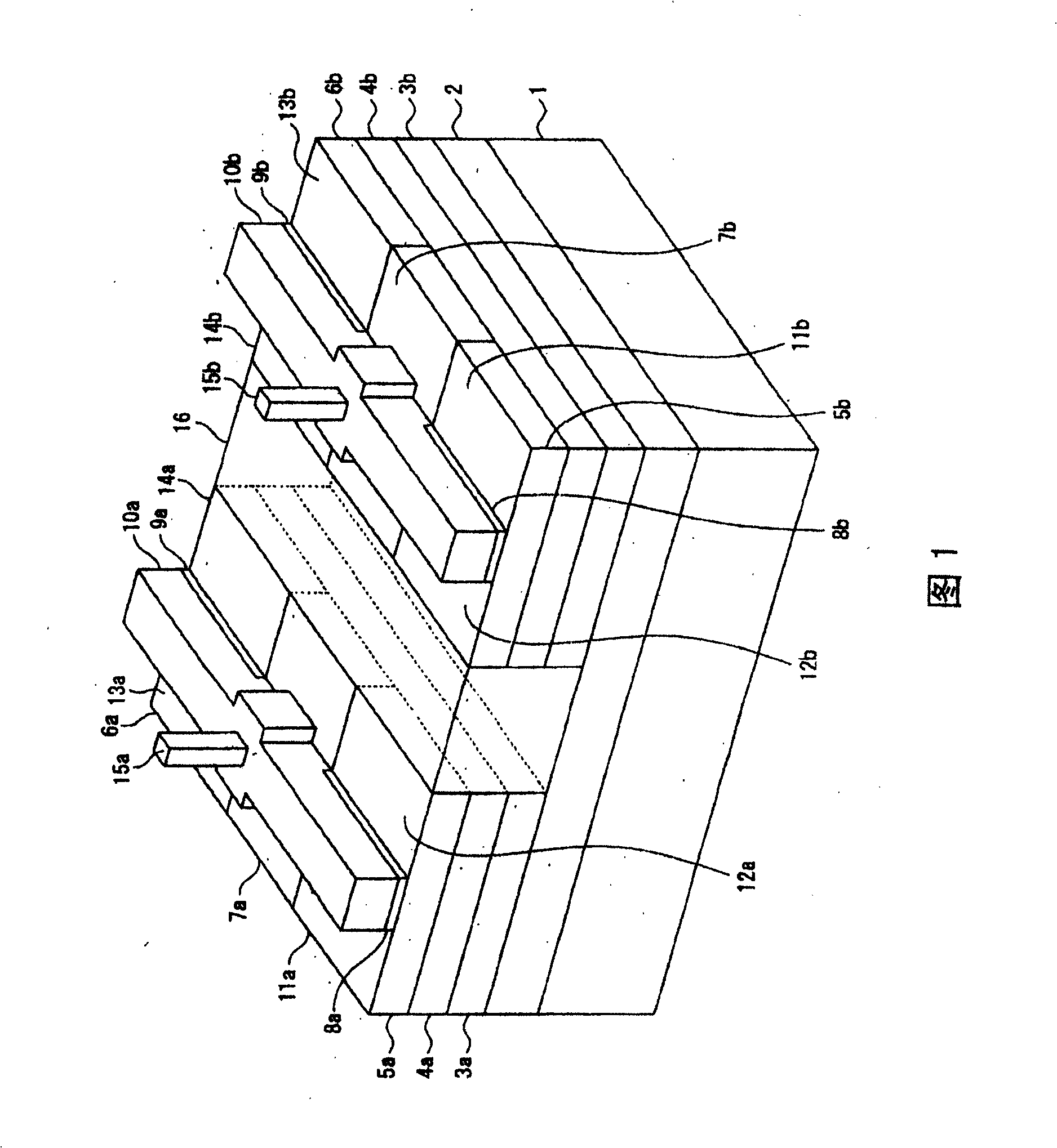
[0046] FIG. 1 is a perspective view showing a schematic configuration of a semiconductor device according to a first embodiment of the present invention.

[0047] In FIG. 1 , an insulating layer 2 is formed on a semiconductor substrate 1 , and single crystal semiconductor layers 3 a and 3 b separated by mesas are stacked on the insulating layer 2 . Further, the single crystal semiconductor layers 5a, 6a separated by mesas are stacked on the single crystal semiconductor layer 3a via the insulating layer 4a, and the single crystal semiconductor layer 5b separated by the mesas is stacked on the single crystal semiconductor layer 3b via the insulating layer 3b. , 6b. In addition, as materials of the semiconductor substrate 1 and the single crystal semiconductor layers 3a, 3b, 5a, 6a, 5b, and 6b, for e...


PUM


Abstract

A semiconductor device is provided in the invention, wherein a gate electrode 10a arranged across an isolation insulation layer 7a is formed on single crystal semiconductor layers 5a and 6a through gate insulating films 8a and 9a, respectively, a P type source layer 11a and a P type drain layer 12a arranged to sandwich the gate electrode 10a are formed on the single crystal semiconductor layer 5a, an N type source layer 13a and an N type drain layer 14a arranged to sandwich the gate electrode 10a are formed on the single crystal semiconductor layer 6a, and a buried electrode 15a connected with a semiconductor layer 3a while penetrating the gate electrode 10a, the isolation insulation layer 7a and an isolation insulation layer 4a, is formed. Therefore, the invention can form a field plate under a field effect transistor of different conductivity type arranged on an insulator while suppressing increase in chip size.

Description

technical field [0001] The present invention relates to a semiconductor device and a method of manufacturing the semiconductor device, and is particularly preferably applicable to a method of forming a field plate in a field effect transistor having a different conductivity type arranged on an insulator. Background technique [0002] In a conventional semiconductor device, for example, as disclosed in Patent Documents 1 and 2, in order to realize a high withstand voltage of a field effect transistor, a field electrode is formed on an insulating film covering the field effect transistor, and the field electrode method of connection to gate or source. [0003] However, in the conventional field electrode structure, the field electrode is formed on an insulating film covering the field effect transistor. Therefore, it is necessary to dispose the field electrode so as to avoid the contact of the gate electrode or the source / drain, and there is a problem that the breakdown volta...

Claims


Application Information

Patent Timeline
Patent Type & Authority Patents(China)
IPC IPC(8): H01L27/12H01L21/84
Inventor 加藤树理
Owner SEIKO EPSON CORP
Learn More