One-dimensional metal photon dielectric crystal and its design method and application
A metal medium, photonic crystal technology, applied in optics, nonlinear optics, instruments, etc., can solve problems such as restricting applications and complex photonic crystal structures.
- Summary
- Abstract
- Description
- Claims
- Application Information
AI Technical Summary
Problems solved by technology
Method used
Image

Examples
Embodiment 1
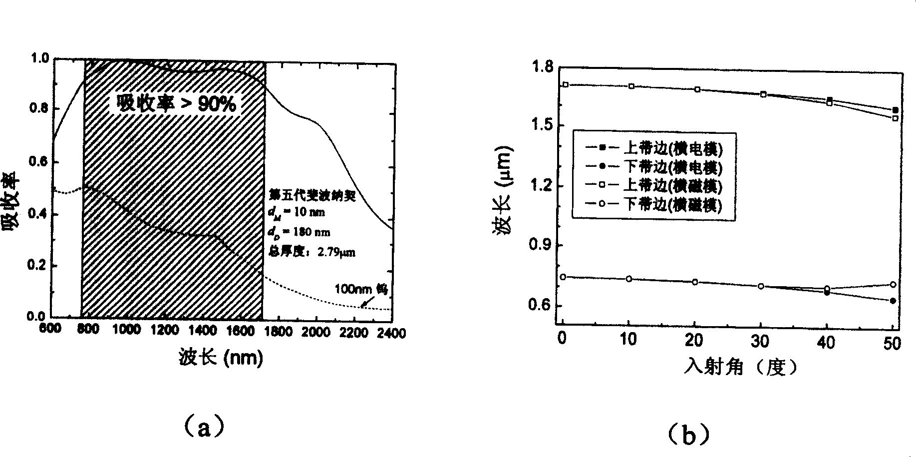
[0023] figure 1 It shows the absorption characteristic diagram of the one-dimensional metal dielectric photonic crystal using the fifth-generation Fibonacci quasi-periodic sequence, which can realize wide incident angle and broadband high absorption. The structure adopts F 5 =(DMDMDDMD) S , where D is n D =1.38 materials (such as SiO 2 ), d D =180nm, M is metal tungsten, d M =10 nm, S=3. figure 1 (a) shows that the spectral band width with an absorption rate above 90% covers a wide frequency band from 0.745 μm to 1.708 μm, and the total thickness is 2.79 μm. figure 1 (b) shows that the high absorption edge of dual-polarized light is almost unchanged in the range of incident angles from 0° to 50°, indicating that the structure has a wide range of angles and can basically meet the needs of large-angle incident angles.
Embodiment 2
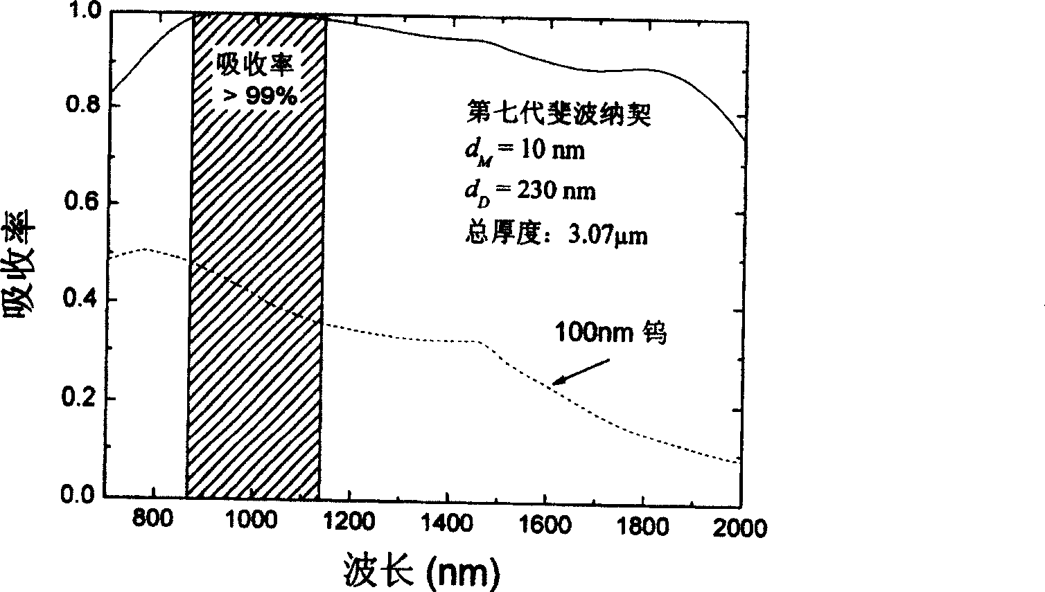
[0025] figure 2 It shows the absorption spectrum diagram of the seventh-generation Fibonacci quasi-periodic one-dimensional metal dielectric photonic crystal, which can realize wide incident angle and broadband high absorption. The structure adopts F 7 =(DMDMDDMDMDDMDDMDMDDMD) S , where S=1, and other parameters are the same as in Example 1. figure 2 It shows that the band width with the absorption rate above 99% covers the frequency band with the center wavelength of 1 μm and the bandwidth from 0.868 μm to 1.133 μm, and the total thickness is 3.07 μm. For the two polarization states of transverse electric mode and transverse magnetic mode, the angle applicable range of the absorption property is 0-50°, which can basically meet the requirement of large-angle incidence.
Embodiment 3
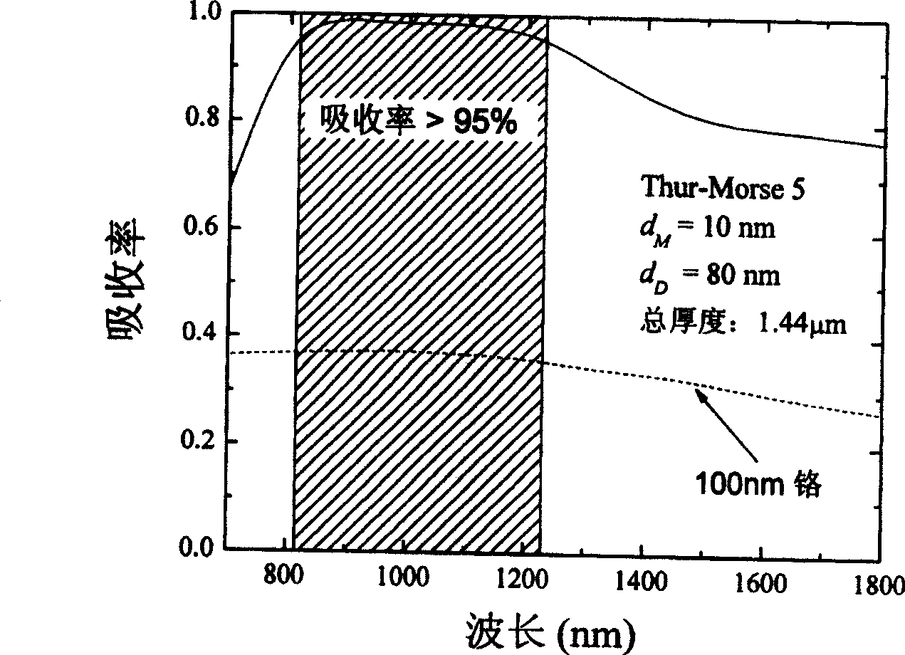
[0027] image 3 It shows the absorption spectrum diagram of the Thue-Morse quasi-periodic one-dimensional metal dielectric photonic crystal to achieve broadband and high absorption at wide incident angles. The structure adopts TM 5 =(DMMDMDDMMDDMDMMDMDDMDMMDDMMDMDDM) S , where D is n D = 2.67 materials (such as GaN), d D =80nm, M is metal chromium, d M = 10 nm. S=1. image 3 It shows that the spectral band width with the absorption rate above 95% covers the frequency band with the center wavelength of 1.024 μm and the bandwidth from 0.817 μm to 1.23 μm, and the total thickness is 1.44 μm. For the two polarization states of transverse electric mode and transverse magnetic mode, the angle applicable range of the absorption property is 0-60°, which can basically meet the requirement of large-angle incidence.
[0028] Embodiments 1 to 3 are examples of structural design of a wide incident angle broadband high absorption one-dimensional metal dielectric photonic crystal. Th...
PUM
 Abstract
Description
Claims
Application Information
 - R&D
- Intellectual Property
- Life Sciences
- Materials
- Tech Scout
- Unparalleled Data Quality
- Higher Quality Content
- 60% Fewer Hallucinations
Browse by: Latest US Patents, China's latest patents, Technical Efficacy Thesaurus, Application Domain, Technology Topic, Popular Technical Reports.
© 2025 PatSnap. All rights reserved.Legal|Privacy policy|Modern Slavery Act Transparency Statement|Sitemap|About US| Contact US: help@patsnap.com