

Grid structure of carbon nano-tube field emission display device and manufacturing method thereof
A carbon nanotube and gate structure technology, applied in the field of field emission display manufacturing, can solve the problems of unfavorable production of large-area display panels, harsh alignment requirements, low yield, etc., to protect the carbon nanotube layer and enhance adhesion , The effect of improving the emission performance
- Summary
- Abstract
- Description
- Claims
- Application Information
AI Technical Summary
Problems solved by technology
Method used
Image

Examples
Embodiment Construction
[0015] specific implementation plan
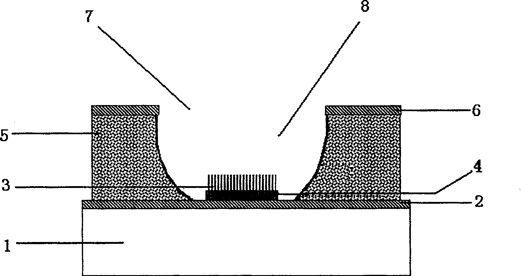
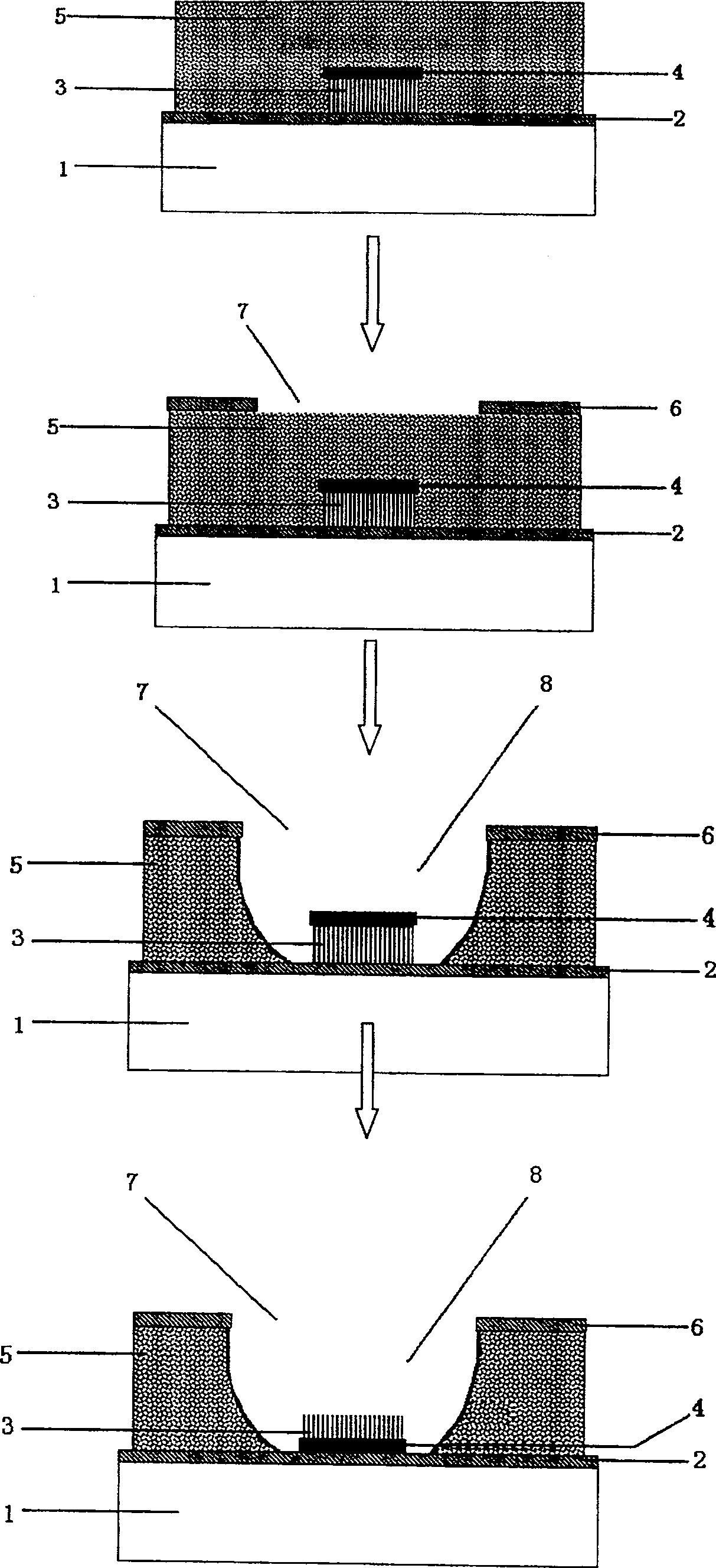
[0016] The method for making the grid structure of the carbon nanotube field emission display device of the present invention proposes the process of making the carbon nanotube slurry layer first, and then making the grid, which avoids the difficulty of accurate alignment, and proposes a corresponding The cathode surface treatment process. The cathode glass substrate is washed with alcohol and deionized water to make a strip-shaped silver electrode as the cathode electrode. After the carbon nanotube raw material is purified and ball-milled, it is mixed into a solution of ethyl cellulose and terpineol in a certain proportion, heated and magnetically The agitator is fully mixed to make printing paste, and the carbon nanotube paste layer pattern is prepared on the cathode electrode by screen printing. Baking to 300°C makes the ethyl cellulose and terpineol in the carbon nanotube slurry decompose and volatilize, and the carbon nanotubes and a...
PUM
| Property | Measurement | Unit |
|---|---|---|
| melting point | aaaaa | aaaaa |
Abstract
Description
Claims
Application Information