Silicon base covariant underlay with the ultrathin carbon silicon middle layer and its preparing method
An interlayer, silicon carbide technology, applied in sustainable manufacturing/processing, climate sustainability, final product manufacturing, etc., can solve problems such as difficulty in realizing 3C-SiC thin films, inability to obtain, etc., and achieve a good mismatch strain coordination effect , to avoid the problem of impurity pollution, the effect of improving the growth quality
- Summary
- Abstract
- Description
- Claims
- Application Information
AI Technical Summary
Problems solved by technology
Method used
Image

Examples
preparation example Construction
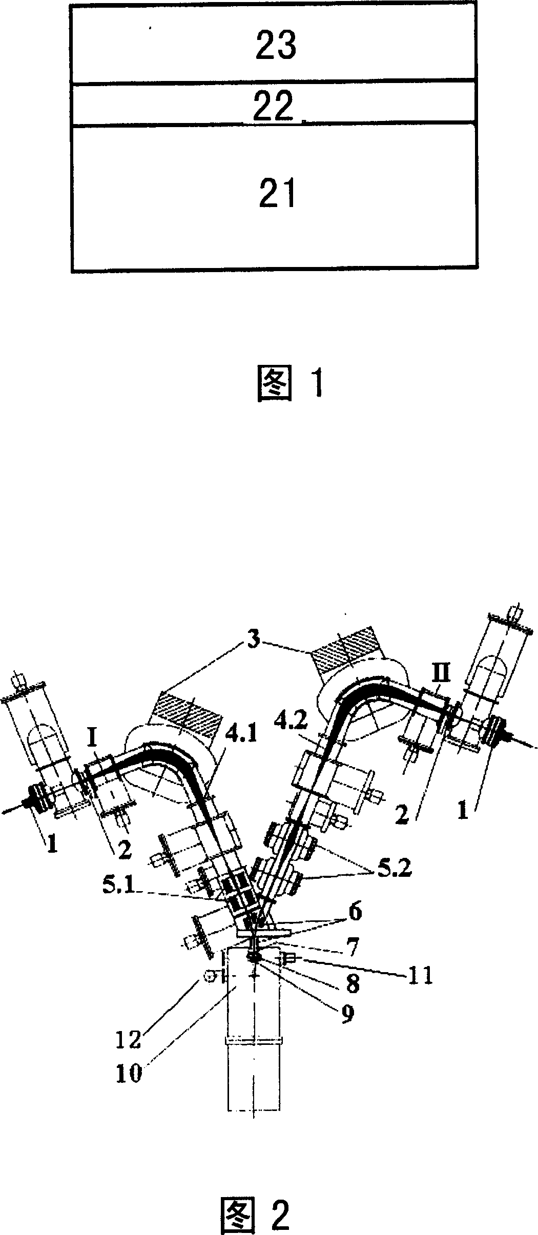
[0048] Please refer to Fig. 1 again, a method for preparing a silicon-based variable substrate with an ultra-thin silicon carbide intermediate layer according to the present invention is characterized in that the preparation method includes the following steps:
[0049] Take a silicon substrate 21;
[0050] Preparing an ultra-thin 3C-SiC intermediate layer 22 on a silicon substrate 21 by ion beam epitaxy;
[0051] An epitaxial layer 23 is prepared on the ultra-thin 3C-SiC intermediate layer 22 by magnetron sputtering.
[0052] The preparation steps of the ultra-thin 3C-SiC intermediate layer 22 are as follows:
[0053] Step 1: Select argon gas with low purity requirements as the I-beam ion source of the low-energy dual ion beam epitaxy equipment to generate argon ion beam raw materials for dry sputtering cleaning of the substrate surface;
[0054] Step 2: Select carbon monoxide gas with low purity requirements as the low-energy dual ion beam epitaxy equipment II beam ion sou...
Embodiment
[0072] The structure of the silicon-based covariable substrate with an ultra-thin silicon carbide interlayer is shown in Figure 1, and its main technical parameters are shown in Table 1.
[0073] Table 1: Main technical parameters of silicon-based variable substrate with ultra-thin silicon carbide interlayer
[0074]
Supporting substrate 21
Material
Silicon (Si)
Thickness (μm)
300-500
crystal quality
Covariant middle layer 22
Material
Cubic silicon carbide (3C-SiC)
Thickness (nm)
5-30
crystal quality
single crystal or polycrystalline
Mismatched Epitaxial Layer 23
Lattice mismatch with substrate 1
Not less than 10%
[0075] crystal with covariable interlayer 2
Not more than 10%
crystal quality
single crystal or polycrystalline
[0076] Referring to the schematic diagram of the S...
PUM
| Property | Measurement | Unit |
|---|---|---|
| thickness | aaaaa | aaaaa |
Abstract
Description
Claims
Application Information
 - Generate Ideas
- Intellectual Property
- Life Sciences
- Materials
- Tech Scout
- Unparalleled Data Quality
- Higher Quality Content
- 60% Fewer Hallucinations
Browse by: Latest US Patents, China's latest patents, Technical Efficacy Thesaurus, Application Domain, Technology Topic, Popular Technical Reports.
© 2025 PatSnap. All rights reserved.Legal|Privacy policy|Modern Slavery Act Transparency Statement|Sitemap|About US| Contact US: help@patsnap.com