Encapsulation structure and method of the high-speed semiconductor light emission component

A technology of light emission components and packaging structures, which is applied in the manufacture of semiconductor devices, semiconductor lasers, semiconductor/solid-state devices, etc., can solve problems such as difficult to achieve high speed, achieve the effect of reducing eccentricity, reducing load, and facilitating debugging and installation

Inactive Publication Date: 2007-08-15
SEMICON MFG INT (SHANGHAI) CORP +1
View PDF0 Cites 37 Cited by
  • Summary
  • Abstract
  • Description
  • Claims
  • Application Information

AI Technical Summary

Problems solved by technology

However, it is difficult for these packages to achieve high speed, especially the transmission rate requirements of 10Gbit / s and higher

Method used


Image

  • Encapsulation structure and method of the high-speed semiconductor light emission component
  • Encapsulation structure and method of the high-speed semiconductor light emission component

Examples


Embodiment Construction

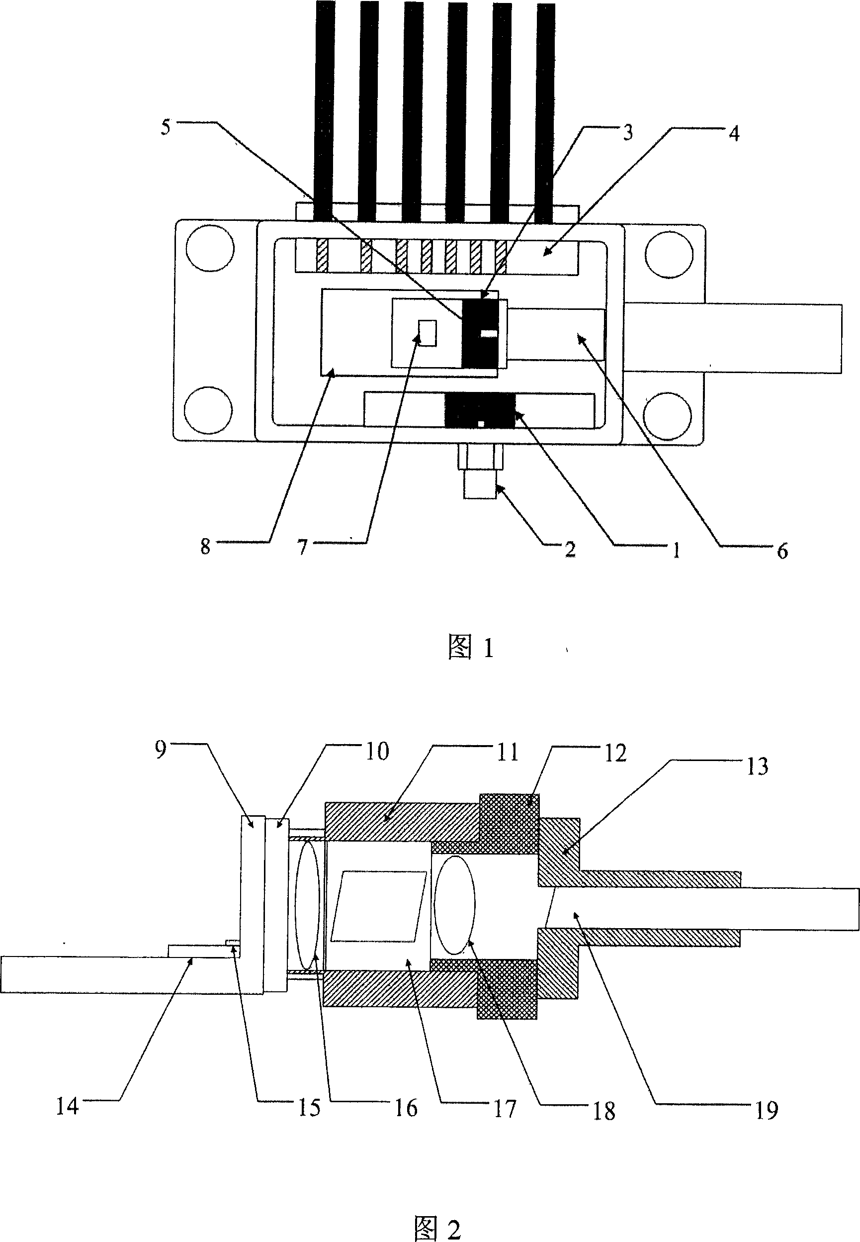
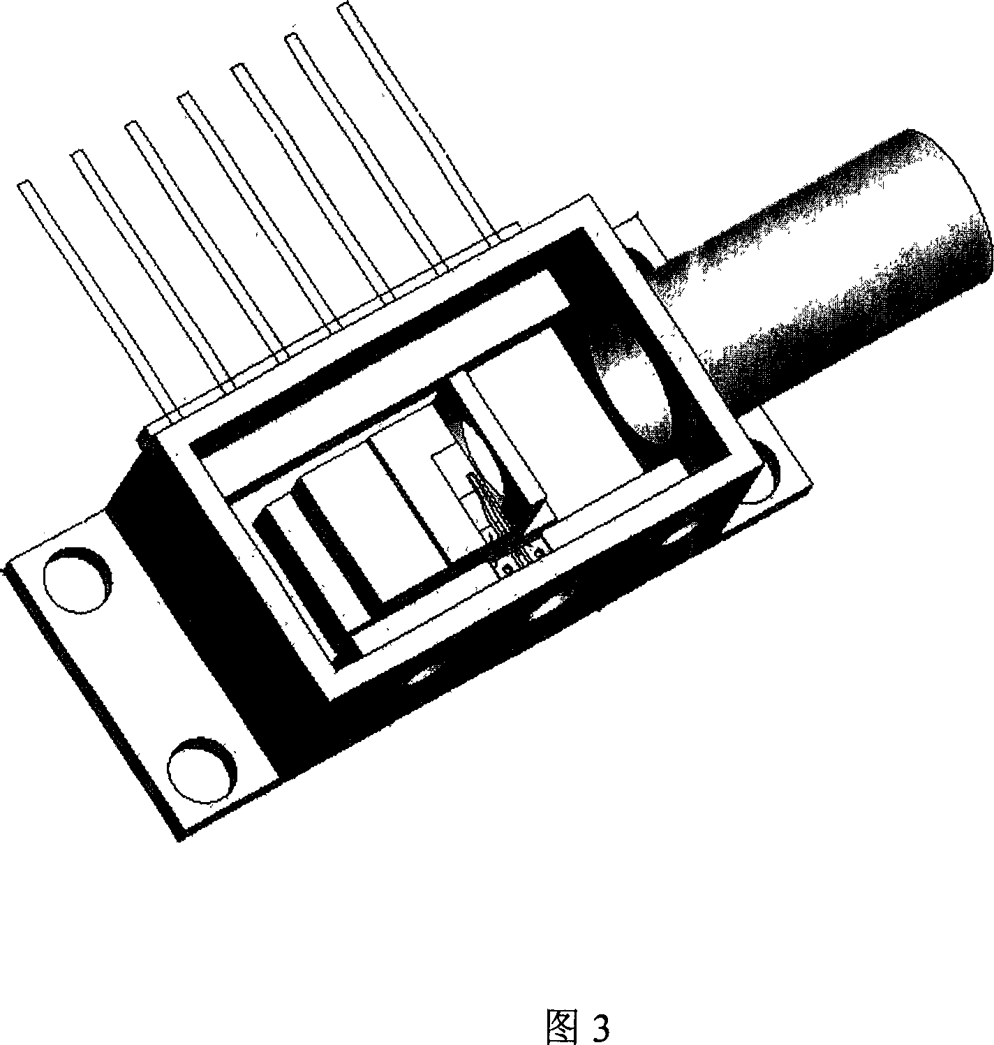
[0044] The packaging structure of the present invention in Fig. 1 uses two separate heat sinks to realize the low-loss input of radio frequency signals from the radio frequency connector to the light emitting device. The two heat sinks are operated separately and finally connected by gold wires or gold ribbons, so that The difficulty of packaging operation is reduced, and the packaging yield is improved. 1 is a dielectric substrate with a coplanar waveguide transmission line (denoted as CPWI) connected to the radio frequency connector; 3 is a coplanar waveguide transmission line (denoted as CPW2) for inputting high-frequency signals to the light emitting device, matching resistors and Dielectric heat sink substrate for DC wiring electrodes; the substrate material can be ceramic materials such as alumina, aluminum nitride, beryllium oxide, high-resistance silicon wafers, etc., but not limited to these; the back of the substrate is metallized and can have sides Metallization and...


PUM


Abstract

The package structure for a high-speed semiconductor light emission assembly comprises: a dish-type case with RF connector, a semiconductor refrigerator to control the work temperature of emission chip, a KOVAR metal heat sink, a medium heat sink substrate, a light emission device, a thermistor, a backlight detector, the metal wire to connect dc connection electrode and case pin, a coplanar waveguide transmission lie on medium substrate, and optical coupling assembly. Wherein, it uses BTF standard package form for dc terminals outside the case.

Description

technical field [0001] The invention mainly relates to the field of optical fiber communication, and more specifically relates to a package structure of a light emitting component for high-speed, long-distance transmission. Background technique [0002] In the field of optical fiber communication, semiconductor lasers and their integrated devices with other optoelectronic devices have always been the preferred devices as signal sources. Here we collectively refer to semiconductor lasers and their integrated devices with other optoelectronic devices as semiconductor light-emitting devices, for example, various semiconductor lasers; integrated devices of DFB / DBR lasers and modulators; lasers, modulators, amplifiers, and spot converters , integrated devices of various functional devices such as optical waveguides, but not limited to these. [0003] After the optoelectronic device chip is manufactured, packaging is the key to whether the device can fully demonstrate its perform...

Claims


Application Information

Patent Timeline
Patent Type & Authority Applications(China)
IPC IPC(8): H01S5/026H01S5/022H01S5/024H01S5/00H01L25/00H01L23/00H01L21/50G02B6/00H04B10/02H04B10/50
Inventor 吴德馨杨成樾李宝霞
Owner SEMICON MFG INT (SHANGHAI) CORP
Why Eureka
Try Eureka