

Constituting method for metal ordered structure surface reinforced base
A technology of ordered structure and surface enhancement, applied in the fields of nanostructure fabrication, Raman scattering, nanotechnology, etc., can solve the problems of expensive instruments, limited application, low efficiency, etc.
- Summary
- Abstract
- Description
- Claims
- Application Information
AI Technical Summary
Problems solved by technology
Method used
Image

Examples
Embodiment 1
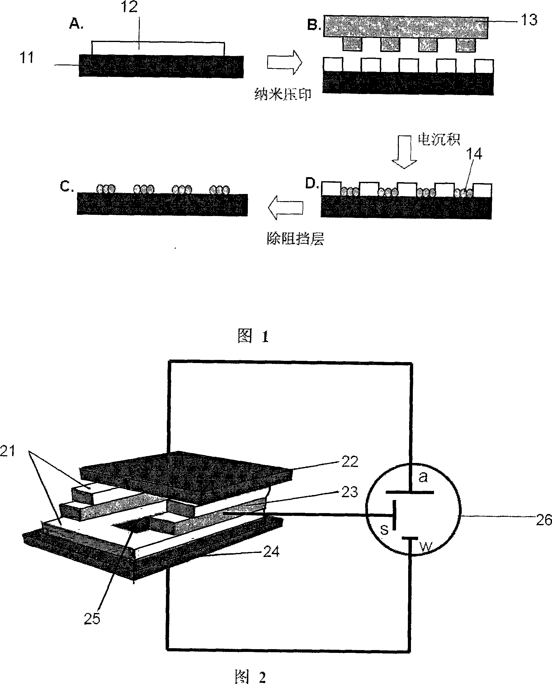
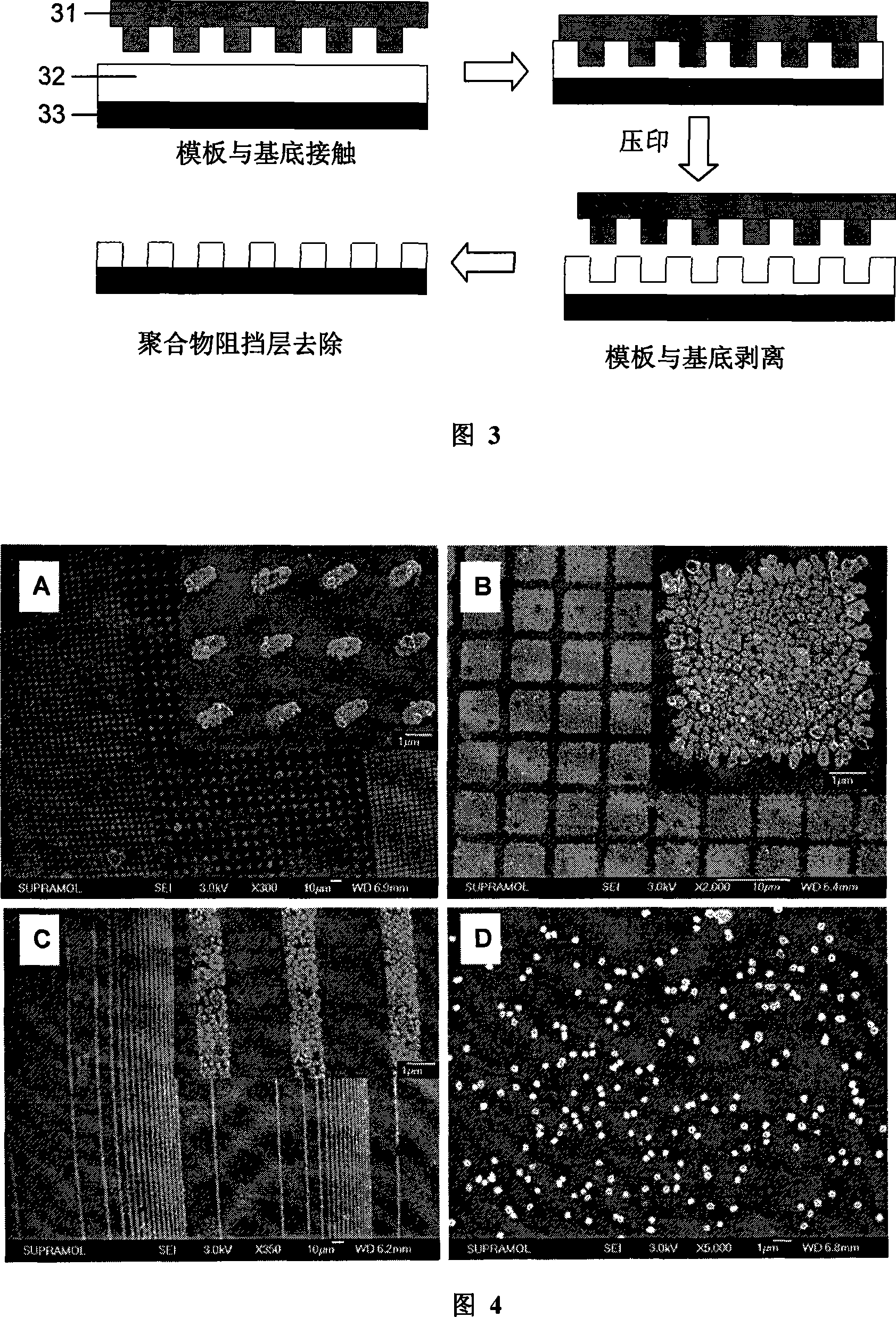
[0091] Take a small amount of thermoplastic polymer MRI-7030 (Micro Resist Company, Germany) and spin-coat it on the treated ITO surface. The spin-coating thickness is about 300nm. Acetone, ethanol and high-purity water were ultrasonically cleaned for 5 minutes, dried with high-purity nitrogen, and then treated with oxygen plasma at a power of 200 mW for 3 minutes to activate the ITO surface. Using the 2.5-inch nano-imprinting machine produced by Sweden's OBDUCAT company, the template of silicon nitride material (constructed by electron beam etching method, its structure is divided into two parts, one part is a lattice structure, the size of the point The range is 800nm×800nm~10μm×10μm, and the pitch size range of dots is 800nm~10μm; the other part is a strip structure, whose line width and line spacing are 800nm~10μm) to build a complementary structure of polymer and template Ordered structure, that is, the use of nanoimprinting method to build microstructures on the surface ...
Embodiment 2
[0095] Take a small amount of polymethyl methacrylate PMMA (sigma-aldrich) and spin-coat it on the treated ITO surface. The spin-coating thickness is about 300nm. Ultrasonic cleaning for 5 minutes, drying with high-purity nitrogen, and using oxygen plasma at a power of 200 mW for 3 minutes to activate the ITO surface. Using the 2.5-inch nano-imprinting machine produced by Sweden's OBDUCAT company, the template of silicon nitride material (constructed by electron beam etching method, its structure is divided into two parts, one part is a lattice structure, the size of the point The range is 800nm×800nm~10μm×10μm, the pitch size range of dots is 800nm~10μm, and the other part is a strip structure, whose line width and line spacing are 800nm~10μm) to build a complementary order of polymer and template structure Structure (one part is a concave dot matrix structure, and its size ranges from 800nm×800nm to 10μm×10μm, and the pitch is 800nm to 10μm; the other part is a strip str...
Embodiment 3
[0097] Spin-coat a small amount of polystyrene PS (sigma-aldrich) on the treated ITO surface with a spin-coating thickness of about 300nm. The treatment method is to cut the ITO into a size of 2cm×2cm, and then use acetone, ethanol and high-purity water to ultrasonically clean it for 5min. , after blowing dry with high-purity nitrogen gas, use oxygen plasma to activate the ITO surface with a power of 200mW for 3min. Using the 2.5-inch nano-imprinting machine produced by Sweden's OBDUCAT company, the template of silicon nitride material (constructed by electron beam etching method, its structure is divided into two parts, one part is a dot matrix structure, the size of the dots The range is 800nm×800nm~10μm×10μm, the pitch size range of dots is 800nm~10μm, and the other part is a strip structure, whose line width and line spacing are 800nm~10μm) to build a complementary order of polymer and template structure Structure (one part is a concave dot matrix structure, and its size r...
PUM
| Property | Measurement | Unit |
|---|---|---|
| Volume | aaaaa | aaaaa |
| Thickness | aaaaa | aaaaa |
| Particle size | aaaaa | aaaaa |
Abstract
Description
Claims
Application Information