Near-ultraviolet or ultraviolet excited semiconductor luminous material and its preparing method

A fluorescent material, yellow-green light technology, applied in the direction of luminescent materials, semiconductor/solid-state device manufacturing, semiconductor devices, etc., can solve the problems of unstable chemical and optical properties, difficult to control reaction conditions, uneven particle size of materials, etc., to achieve high chemical efficiency And the effect of optical stability, easy operation of production process, and improvement of luminous intensity

Inactive Publication Date: 2007-08-29
SHANGHAI NORMAL UNIVERSITY
View PDF0 Cites 8 Cited by
  • Summary
  • Abstract
  • Description
  • Claims
  • Application Information

AI Technical Summary

Problems solved by technology

[0005] The technical problem to be solved by the present invention is to provide a semiconductor luminescent material excited by near-ultraviolet or ultraviolet light and its preparation method, so as to overcome the high price of raw materials, complicated preparation steps, difficult control of reaction conditions and the large particle size of the obtained material in the original method. Uniformity, chemical and optical properties are not stable enough, and the defects of low luminous efficiency

Method used


Image

  • Near-ultraviolet or ultraviolet excited semiconductor luminous material and its preparing method
  • Near-ultraviolet or ultraviolet excited semiconductor luminous material and its preparing method
  • Near-ultraviolet or ultraviolet excited semiconductor luminous material and its preparing method

Examples


Embodiment 1

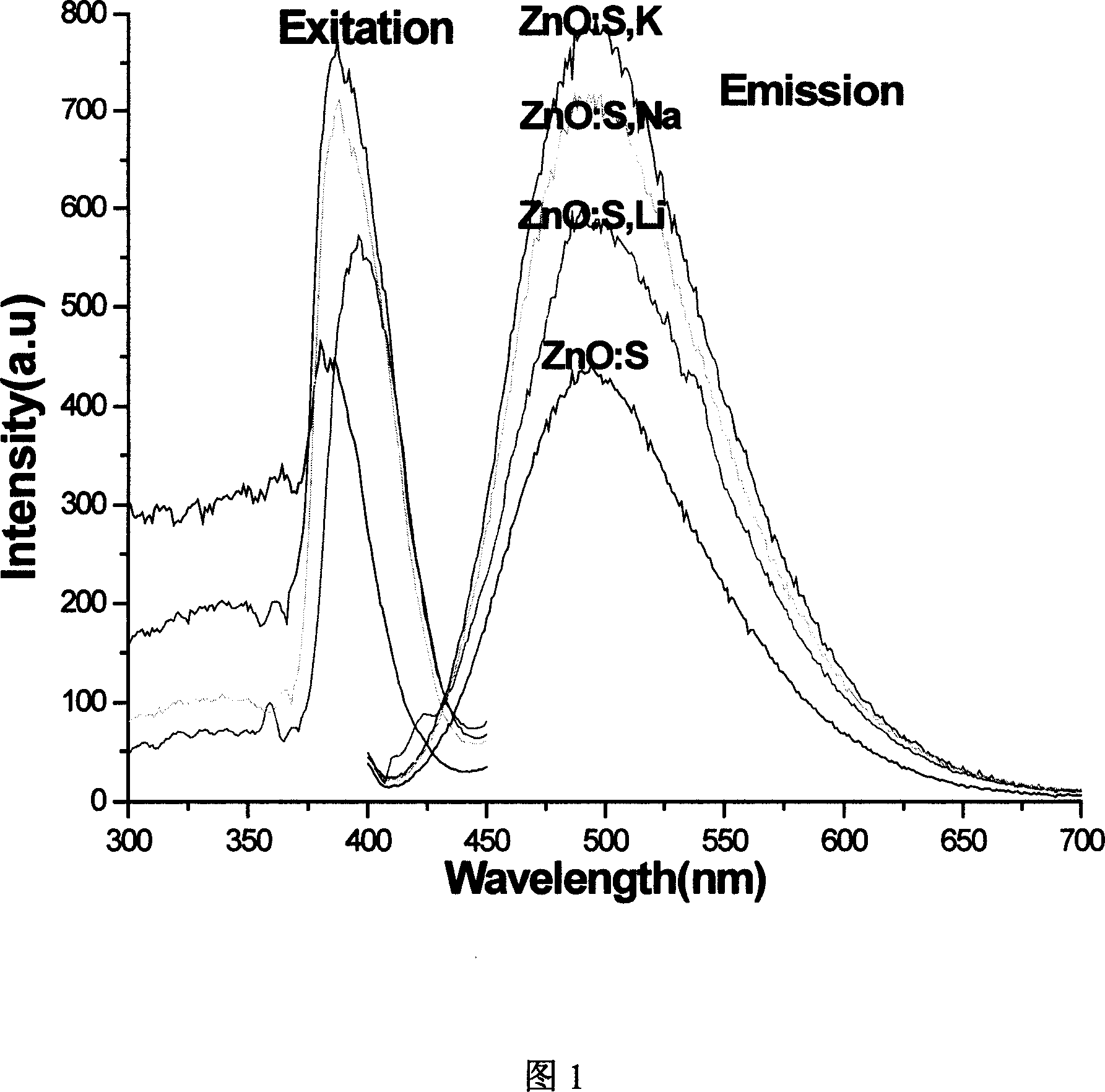
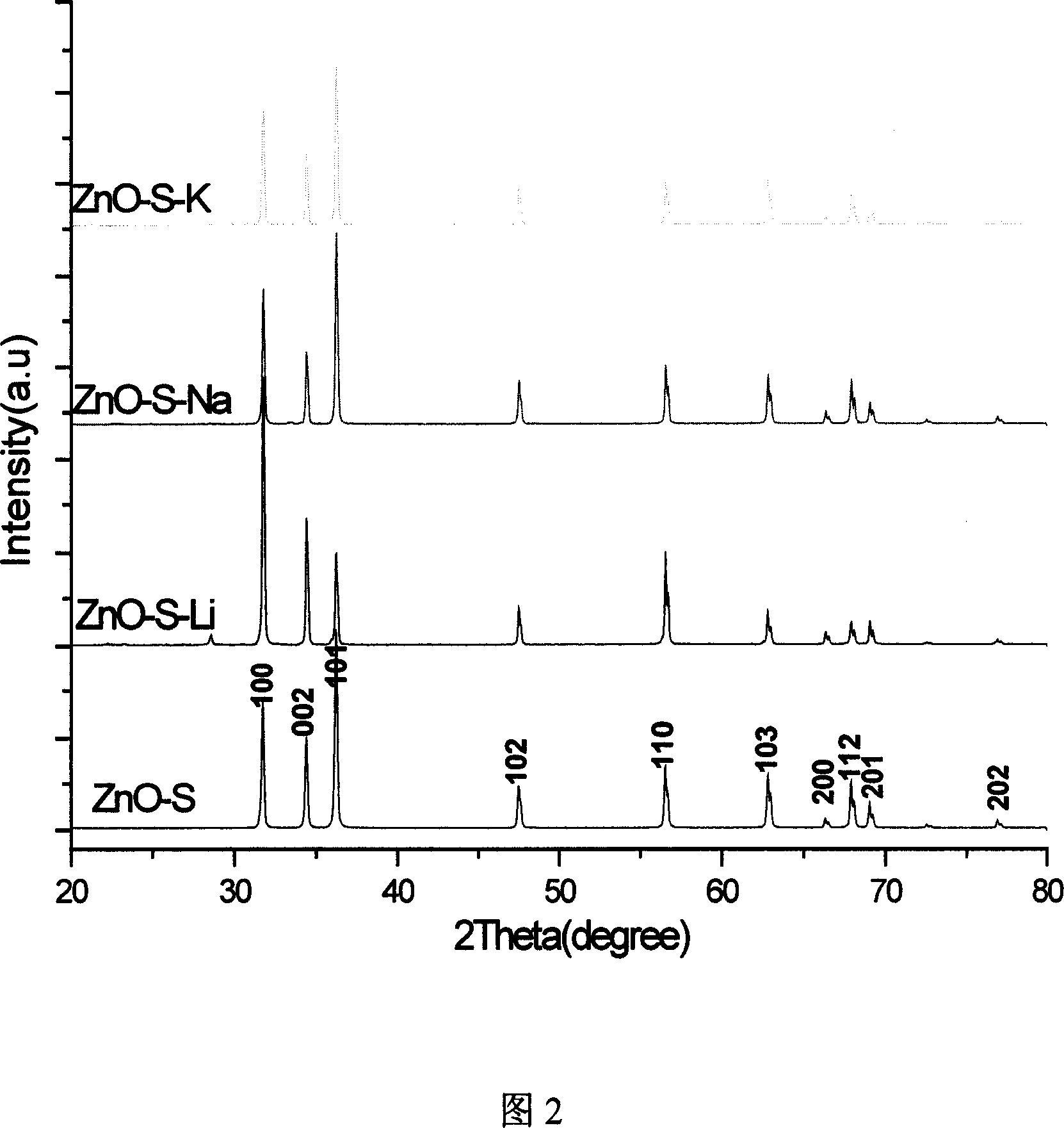
[0040] Weigh 9.7g of ZnS and 0.6030g of NaCl, add them to 50mL of ethanol solution, stir in a water bath at 65°C for 10 minutes, then ultrasonically disperse for 5 minutes, keep heating in a water bath at 65°C and continue stirring for 30 minutes, then distill off the ethanol under reduced pressure at 70°C to obtain a precursor The above precursors were sintered in a muffle furnace at 850°C for 2 hours and then ground slightly to obtain the target product.

Embodiment 2

[0042] Weigh 9.7g ZnS and 0.6042g LiCl.H2O, add to 50mL ethanol solution, stir in 65°C water bath for 10min, then ultrasonically disperse for 5min, keep stirring in 65°C water bath for 30min, then remove ethanol by distillation under reduced pressure at 70°C To obtain the precursor, put the above precursor in a muffle furnace for sintering at 850°C for 2 hours, and then grind it a little to obtain the target product.

Embodiment 3

[0044] Weigh 9.7g of ZnS and 0.7455g of KCl, add them into 50mL of ethanol solution, stir in a water bath at 65°C for 10 minutes, then ultrasonically disperse for 5 minutes, keep heating in a water bath at 65°C and continue to stir for 30 minutes, then distill off ethanol under reduced pressure at 70°C to obtain a precursor The above precursors were sintered in a muffle furnace at 850°C for 2 hours and then ground slightly to obtain the target product.


PUM


Abstract

The invention discloses a semiconductor emitting material that is stimulated by near ultraviolet or ultraviolet. The constituents are ZnO: Sx, My and 10-4<=x<=10-2, 0<=y<=0.2. M is selected from Li, Na, K or rare earth of Eu, Tb. When M is Na, it has better emitting effect. The invention also discloses the manufacture method and the performance testing result. The invention has strong absorption near 370-440nm wavelength ultraviolet and blue light zone, and has strong emission between 450-600nm wavelengths. It could be used in LED and LD.

Description

technical field [0001] The invention belongs to the field of luminescent materials, and more specifically relates to the field of semiconductor luminescent materials. Background technique [0002] In recent years, with the wide application of various functional materials, the research on the luminescent properties of materials has been deepened. At the same time, due to the most potential of yellow-green light-emitting devices (LEDs), laser diodes (LDs), vacuum fluorescent displays (VFDs) and recent new developments The huge market demand such as field emission flat panel displays (FEDs) has promoted the research on III-V and II-VI semiconductor materials. The unique optical properties of nano-semiconductor materials make them possible to have new potential applications in the field of optoelectronics, and become an important branch of research in the field of material luminescence. ZnO is an important semiconductor material. It is not easy to be oxidized in the atmosphere ...

Claims


Application Information

Patent Timeline
Patent Type & Authority Applications(China)
IPC IPC(8): C09K11/56C09K11/84H01L51/54G09F13/20
Inventor 余锡宾周平乐
Owner SHANGHAI NORMAL UNIVERSITY
Why Eureka
Try Eureka