High-voltage MOSFET device

A high-voltage and device technology, applied in the direction of electric solid devices, semiconductor devices, electrical components, etc., can solve the problems that high-voltage transistors cannot be directly transferred and cannot be used to reduce the gate fringe electric field, etc., to achieve high breakdown voltage, production The effect of low cost and low process complexity

Inactive Publication Date: 2007-09-05
韩小亮
View PDF0 Cites 10 Cited by
  • Summary
  • Abstract
  • Description
  • Claims
  • Application Information

AI Technical Summary

Problems solved by technology

The lack of a thick field oxygen region means that this slab technique cannot be used to reduce the electric field at the gate edge
Thi

Method used


Image

  • High-voltage MOSFET device
  • High-voltage MOSFET device
  • High-voltage MOSFET device

Examples


Embodiment Construction

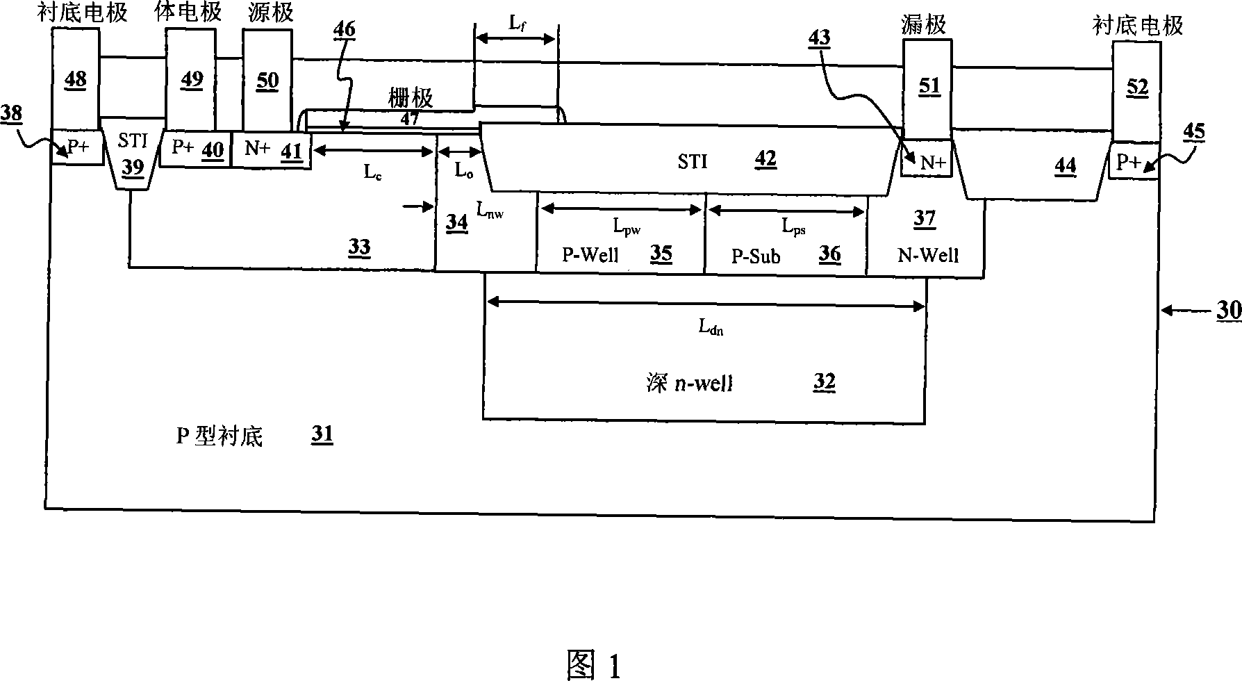
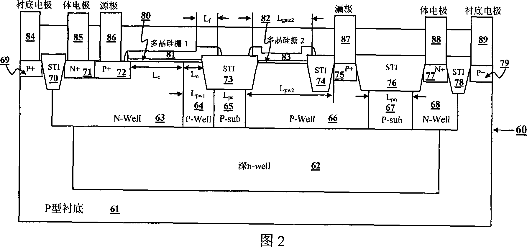
[0026]This new high-voltage NMOS structure is fully usable in standard submicron CMOS processes without changing any existing process steps. Body breakdown instead of silicon surface breakdown, breakdown resistance and reliability are all based on specially designed high-voltage device structures. The proposed HV NMOS structure uses a first n-well, a deep n-well, and a second n-well to create a buffer region between the channel and drain. The breakdown voltage is determined by the impurity concentrations of the first n-well, second p-well, deep n-well and p-type substrate. The surface impurity concentration of the first n-well is lower than that of the n-LDD of the low voltage device. The high breakdown voltage depends on the lateral extension of the first n-well under the gate, as shown by Lo. The second p-well is implanted close to the first n-well to achieve charge compensation, and the length of the compensation region depends on the process design criteria of the used p...


PUM

PropertyMeasurementUnit
Lengthaaaaaaaaaa
Lengthaaaaaaaaaa
Lengthaaaaaaaaaa

Abstract

The invention is concerned with high voltage MOSFET device. There is deep n-wells on P or N tape underlay, at least the first n-well, the second n-well and the first and second p-well, and n-well and p-well have n+ adulteration area or p+ adulteration area, and the source or drain is leading from n+ adulteration area or p+ adulteration area. Usually, grid is leading from poly Si gate covering the thin gate oxide area of n-well or p-well, and there is at least one STI low groove insulation coating between source and drain, while poly Si gate extends to STI area. There is a layer low impurity p type underlay between high voltage drain and the second p-well to prevent the possible breakdown. The high voltage MOSFET device isolated with low groove can combine the breakdown protection characteristics to normal submicron CMOS without changing existing CMOS process.

Description

technical field [0001] The present invention relates to a high-voltage transistor, especially a high-voltage MOSFET (metal oxide semiconductor field effect) device with shallow trench isolation; especially a new high-voltage NMOSFET (metal oxide semiconductor field effect) containing an extended drain based on a standard submicron CMOS process. semiconductor field effect transistor) structure. Background technique [0002] The invention relates to a high-voltage transistor, in particular to a new high-voltage NMOSFET (metal oxide semiconductor field effect transistor) structure with an extended drain and a new high-voltage PMOSFET structure with an extended drain under a standard submicron CMOS process. The purpose of the present invention is to incorporate breakdown resistance into standard sub-micron CMOS without changing the existing CMOS process (only mask control technology is used). The new high-voltage NMOS and PMOS with extended drain can...

Claims


Application Information

Patent Timeline
IPC IPC(8): H01L29/78H01L27/04H01L27/092
Inventor 韩小亮王非
Owner 韩小亮
Why Eureka
Try Eureka