

Epoxy resin composition and semiconductor device
A technology of epoxy resin and semiconductor, which is applied in the direction of semiconductor devices, semiconductor/solid-state device components, electric solid-state devices, etc., and can solve problems such as reduced adhesion, excessive compounding amount, and poor reliability of packages
- Summary
- Abstract
- Description
- Claims
- Application Information
AI Technical Summary
Problems solved by technology
Method used
Image

Examples
Embodiment
[0149] Examples of the present invention are shown below, but the present invention is not limited by these Examples. The compounding ratio is expressed in parts by weight.
[0150] Next, the embodiment series (1) relates to the first aspect, the embodiment series (2) relates to the second aspect, and the embodiment series (3) relates to the third aspect.
[0151] Example series (1)
Embodiment (1
[0153] After mixing each component shown below with a mixer, it kneaded with the twin roll whose surface temperature was 95 degreeC and 25 degreeC, after cooling, it grind|pulverized, and the epoxy resin composition was obtained. The properties of the obtained epoxy resin composition were evaluated by the following methods. The results are shown in Table 1.
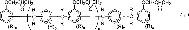
[0154] Epoxy resin 1: Epoxy resin represented by formula (1a) (softening point is 44° C., epoxy equivalent is 234, hereinafter referred to as E-1) 6.21 parts by weight
[0155]
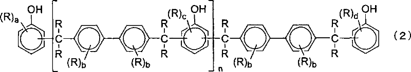
[0156] Phenolic resin 1: phenolic resin represented by formula (2a) (softening point: 107°C, hydroxyl equivalent: 203, hereinafter referred to as H-1) 4.89 parts by weight
[0157]
[0158] 1. 8-diazabicyclo(5,4,0)undecene-7 (hereinafter referred to as DBU)
[0159] 0.20 parts by weight
[0160] Fused spherical silica (average particle size: 25 μm) 88.00 parts by weight
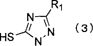
[0161] 1,2,4-triazole-5-...
Embodiment (2
[0194] After mixing each component shown below with a mixer, it kneaded with the twin-roller whose surface temperature was 95 degreeC and 25 degreeC, after cooling, it grind|pulverized, and the epoxy resin composition was obtained. The properties of the obtained epoxy resin composition were evaluated in the following manner. The results are shown in Table 4.
[0195] Epoxy resin 1: Epoxy resin represented by formula (1a) (softening point 44° C., epoxy equivalent 234, hereinafter referred to as E-1) 6.09 parts by weight
[0196]
[0197]Phenolic resin 1: phenolic resin represented by formula (2a) (softening point 107°C, hydroxyl equivalent 203, hereinafter referred to as H-1) 4.41 parts by weight
[0198]
[0199] Organopolysiloxane represented by formula (4a) (hereinafter referred to as organopolysiloxane 1)
[0200] 0.20 parts by weight
[0201]
[0202] Oxidized polyethylene wax 1 (oxidized high-density polyethylene with a dr...
PUM
| Property | Measurement | Unit |
|---|---|---|
| softening point | aaaaa | aaaaa |
| particle size | aaaaa | aaaaa |
| particle size | aaaaa | aaaaa |
Abstract
Description
Claims
Application Information