Semiconductor laser device and manufacturing method thereof
A technology of laser devices and manufacturing methods, applied in the direction of semiconductor laser devices, semiconductor lasers, laser devices, etc., capable of solving problems such as reducing the reliability of active layers
- Summary
- Abstract
- Description
- Claims
- Application Information
AI Technical Summary
Problems solved by technology
Method used
Image

Examples
Embodiment 1
[0058] Dual wavelength semiconductor laser device
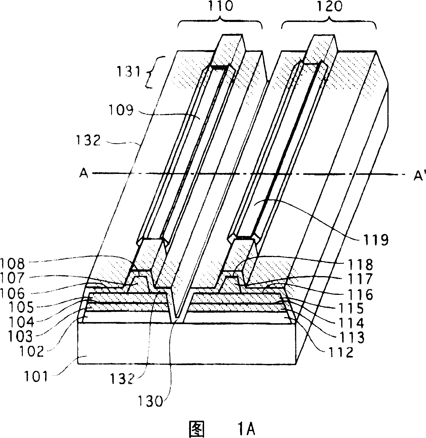
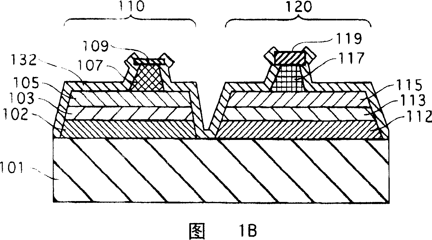
[0059] FIG. 1A is a schematic oblique view of a semiconductor laser device according to Embodiment 1 of the present invention. FIG. 1B is a cross-sectional view of FIG. 1A along line A-A'.
[0060] According to this embodiment, the monolithic dual-wavelength semiconductor laser device consists of an n-type GaAs substrate 101 and an infrared laser unit 110 and a red laser unit 120 mounted on the substrate 101 . Each laser unit has the following configuration.
[0061] The infrared laser unit 110 has the following layers laminated on the n-type GaAs substrate 101 in the order described: n-type GaAs buffer layer 102; n-type (Al x Ga 1-x ) y In 1-y P cladding layer 103; Active layer 104 based on GaAs / AlGaAs; p-type (Al x Ga 1-x ) y In 1-y P first cladding layer 105; p-type GaInP etch stop layer 106; p-type (Al x Ga 1-x ) y In 1-y P second cladding layer 107; p-type GaInP intermediate layer 108; and p-type GaAs contac...
Embodiment 2
[0118] Fig. 6A is a perspective view of a semiconductor laser device according to Embodiment 2 of the present invention. 6B and 6C are cross-sectional views of the semiconductor laser device.
[0119] The semiconductor laser device of Embodiment 2 is basically similar in structure to the semiconductor laser device of Embodiment 1. The difference is that the current blocking layer is made of AlInP. In addition, the manufacturing method is also different from Example 1. The second manufacturing method is described below with reference to FIGS. 5 and 6 .
[0120] Through the same steps shown in FIGS. 2A-3B of Embodiment 1, the ridges constituting the partial waveguide were formed.
[0121] Next, as shown in Figure 5A, photolithography is used to etch the SiO 2 Thin films (not shown) and contact layers 309 and 319 are removed to remove regions where they exist above window structure 331 .
[0122] Next, as shown in FIG. 5B, AlInP is selectively grown to form the current block...
PUM
| Property | Measurement | Unit |
|---|---|---|
| Thickness | aaaaa | aaaaa |
| Carrier density | aaaaa | aaaaa |
| Thickness | aaaaa | aaaaa |
Abstract
Description
Claims
Application Information
 - R&D
- Intellectual Property
- Life Sciences
- Materials
- Tech Scout
- Unparalleled Data Quality
- Higher Quality Content
- 60% Fewer Hallucinations
Browse by: Latest US Patents, China's latest patents, Technical Efficacy Thesaurus, Application Domain, Technology Topic, Popular Technical Reports.
© 2025 PatSnap. All rights reserved.Legal|Privacy policy|Modern Slavery Act Transparency Statement|Sitemap|About US| Contact US: help@patsnap.com