Surface-mounting ceramic electronic component

A technology for ceramic electronic components and electronic components, which is applied to electrical components, resistor components, fixed capacitor components, etc., and can solve problems such as cracks, lack of ductility, and difficulty in resisting impact wiring substrate deflection and falling.

Inactive Publication Date: 2007-10-10
TAIYO YUDEN KK
View PDF1 Cites 52 Cited by
  • Summary
  • Abstract
  • Description
  • Claims
  • Application Information

AI Technical Summary

Problems solved by technology

[0004] In this way, surface-mount ceramic electronic components are composed of ceramics and metals, so they lack ductility, and it is difficult to withstand strong external forces such as impact caused by the mounting device during mounting, deflection of the wiring board after mounting, and falling, and defects such as cracks may occur

Method used


Image

  • Surface-mounting ceramic electronic component
  • Surface-mounting ceramic electronic component
  • Surface-mounting ceramic electronic component

Examples


Embodiment 1

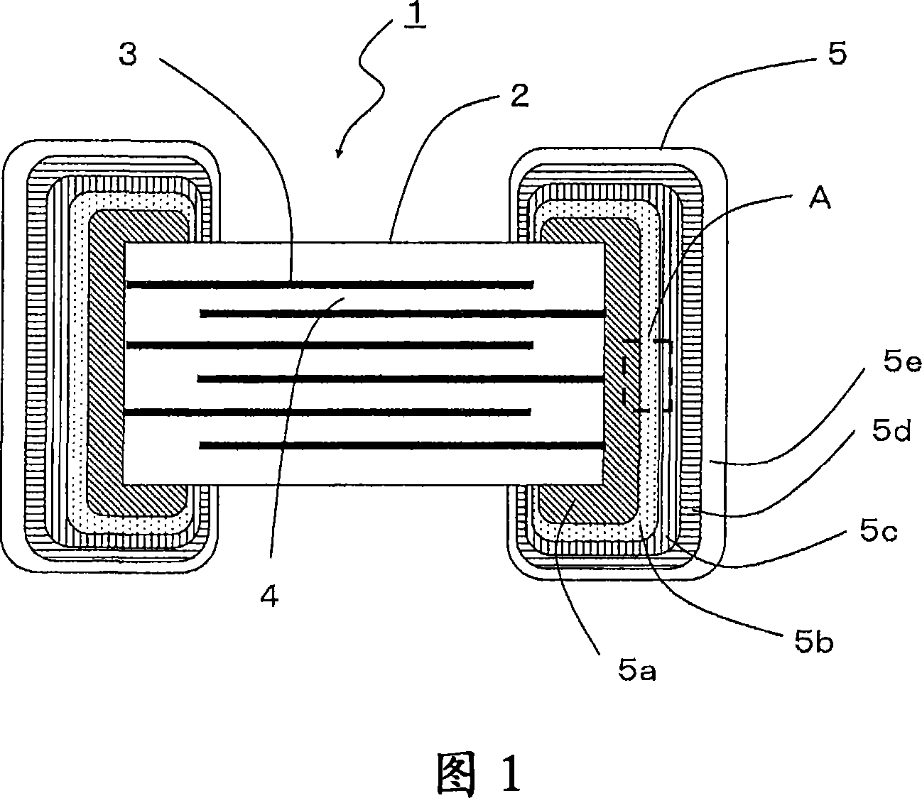
[0034] Dielectric ceramic powder having temperature characteristics representing JIS BJ characteristics was mixed with polyvinyl butyral, its additives, and a solvent to form a mixed slurry, which was formed into a ceramic green sheet having a thickness of 5 μm by a doctor blade. Next, a Ni conductive paste was applied by screen printing on the ceramic green sheet to form internal electrodes. This ceramic green sheet was punched out to a predetermined size, stacked so that the internal electrodes had 10 layers, and bonded by thermocompression to obtain a laminated body. This laminated body was cut into a size of 4.0×2.0 mm. Dip-coat the Ni conductive paste containing the common material on the exposed surface of the internal electrode of the cut laminate, and sinter it in a nitrogen-hydrogen gas at 1300°C to obtain a 3.2×1.6mm-sized substrate with a base metal layer. Multilayer ceramic capacitor basic body.

[0035] A Cu intermediate metal layer having a thickness of 3 μm an...

Embodiment 2

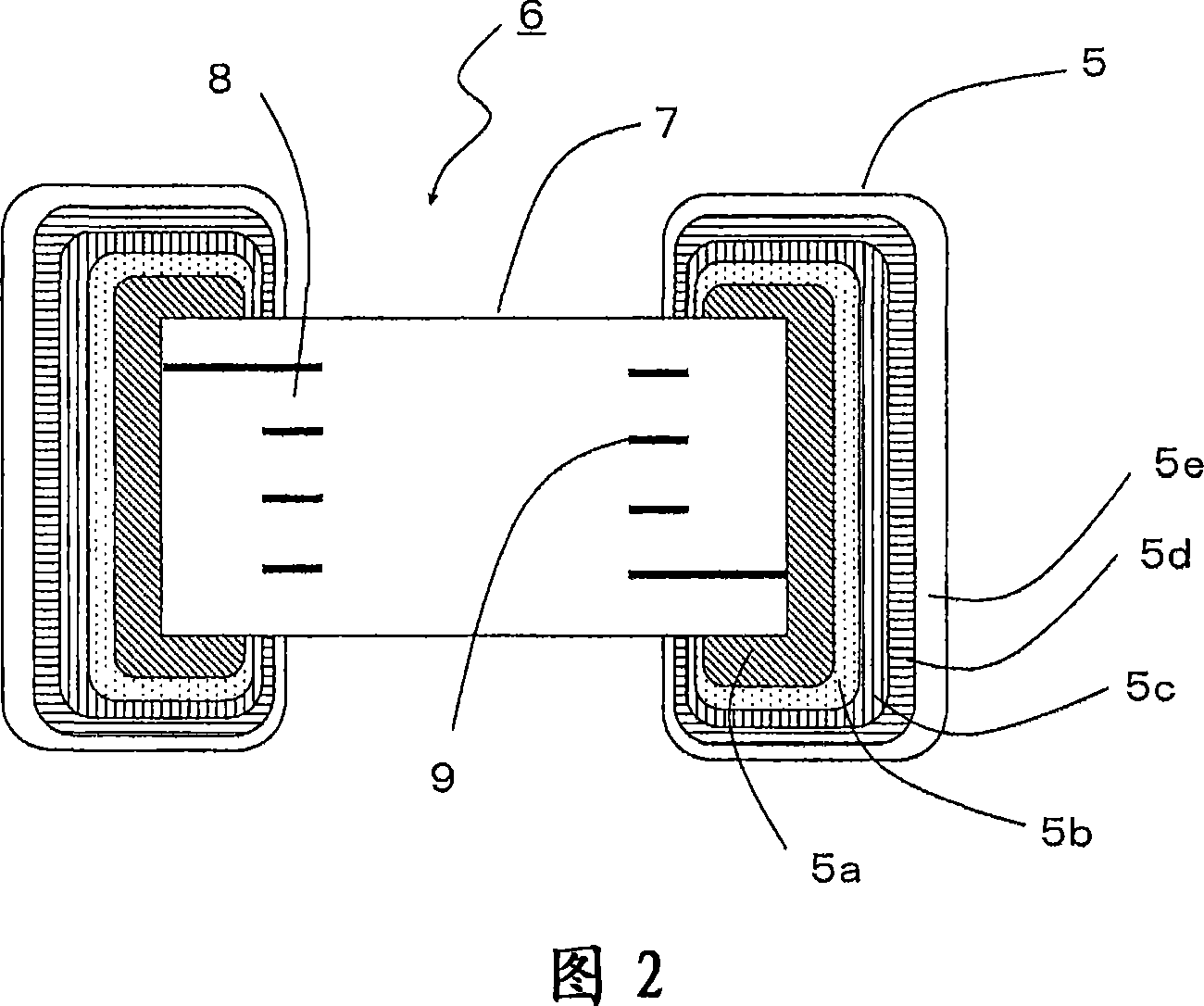
[0037] The same multilayer ceramic capacitor basic body as in Example 1 was prepared, and a Ni intermediate metal layer with a thickness of 3 μm and a continuity rate of 100% was formed on the base metal layer by electrolytic plating. Next, on the Ni intermediate metal layer, the conductive resin filled with Ag in the epoxy resin was impregnated and coated in the same manner as in Example 1, and cured at 200° C. to form a conductive resin layer. A nickel-plated metal layer and a tin-plated metal layer are sequentially formed on the resin layer by electrolytic plating.

Embodiment 3

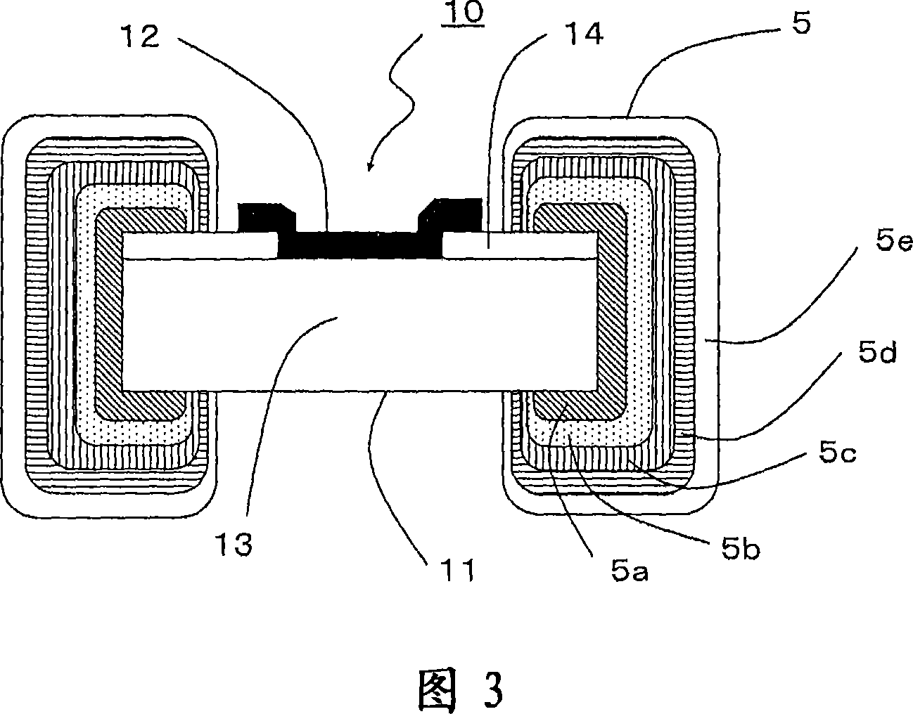
[0044] Prepare the same laminated ceramic capacitor basic body as in Example 1, adjust the plating time on the base metal layer by electrolytic plating, and form Cu intermediate metal layers with film thicknesses of 0.3 μm, 0.5 μm, 1 μm, and 3 μm (continuity ratio: 100 %) of the test material. On the Cu intermediate metal layer of these test materials, a conductive resin layer, a nickel-plated metal layer, and a tin-plated metal layer were sequentially formed in the same manner as in Example 1.

[0045] Ten of these test materials and the test material of Comparative Example 1 were respectively prepared, and a flexure test was performed in accordance with the procedure of JIS-C5101 substrate bending resistance test method. The amount of deflection when the capacitance decreased by 10% or more was measured, and the average value of 10 test materials of each type was calculated. Table 1 shows the results. Even when the amount of deflection was 10 mm, the case where no decrease...


PUM

PropertyMeasurementUnit
thicknessaaaaaaaaaa
sizeaaaaaaaaaa
thicknessaaaaaaaaaa

Abstract

One inventive aspect relates to a surface-mounting ceramic electronic component including a terminal electrode structure which improves the mechanical strength of the electronic component. In the terminal electrode structure, an intermediate metal layer is formed on a base metal layer, and a conductive resin layer is formed thereon. A surface of the base metal layer in which a common material, an oxide film, glass frit or the like exists is covered with the intermediate metal layer, and the conductive resin layer is adhered to the intermediate metal layer as a tight metal surface.

Description

technical field [0001] The present invention relates to surface mount type ceramic electronic components such as ceramic capacitors, laminated inductors, chip resistors, chip varistors, chip thermistors and capacitor arrays, and more particularly to the structure of terminal electrodes (external electrodes). Background technique [0002] In recent years, with the miniaturization of electronic equipment, more and more surface mount electronic components that are conducive to high-density mounting have been adopted. As shown in FIG. 5 , the surface mount type ceramic electronic component 19 is directly mounted on the wiring board 20 by a mounting device, and fixed by reflow soldering or the like. As such surface mount ceramic electronic components, there are multilayer ceramic capacitors, multilayer inductors, chip resistors, chip varistors, and chip thermistors in which a pair of terminal electrodes are formed on a square electronic component base body. components; and compo...

Claims


Application Information

Patent Timeline
Patent Type & Authority Applications(China)
IPC IPC(8): H01G4/30H01G4/005H01G4/008H01C7/00H01C7/18H01F17/00
CPCH01G4/232H01C1/148H01G4/2325
Inventor 齐藤贤二柴崎正二
Owner TAIYO YUDEN KK
Why Eureka
Try Eureka