Self-adaptable package for designing on-chip network

An on-chip network and self-adaptive technology, applied in the direction of data exchange network, digital transmission system, electrical components, etc., can solve the problems of wasting network capacity and increasing the power consumption of on-chip network

Inactive Publication Date: 2007-11-21
TSINGHUA UNIV
View PDF0 Cites 10 Cited by
  • Summary
  • Abstract
  • Description
  • Claims
  • Application Information

AI Technical Summary

Problems solved by technology

[0005] The purpose of the present invention is to propose a self-adaptive packaging method for network on chip design, to overcome the shortcomings of wasting network capacity and increasing power consumption of network on chip in the current fixed-length packaging method

Method used


Image

  • Self-adaptable package for designing on-chip network
  • Self-adaptable package for designing on-chip network
  • Self-adaptable package for designing on-chip network

Examples


Embodiment approach

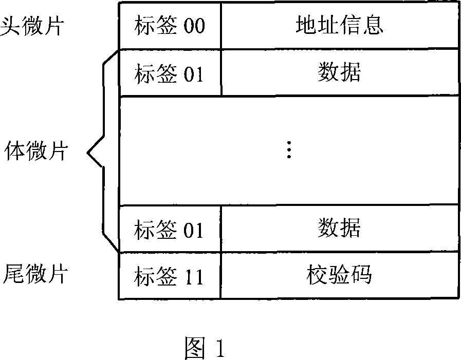
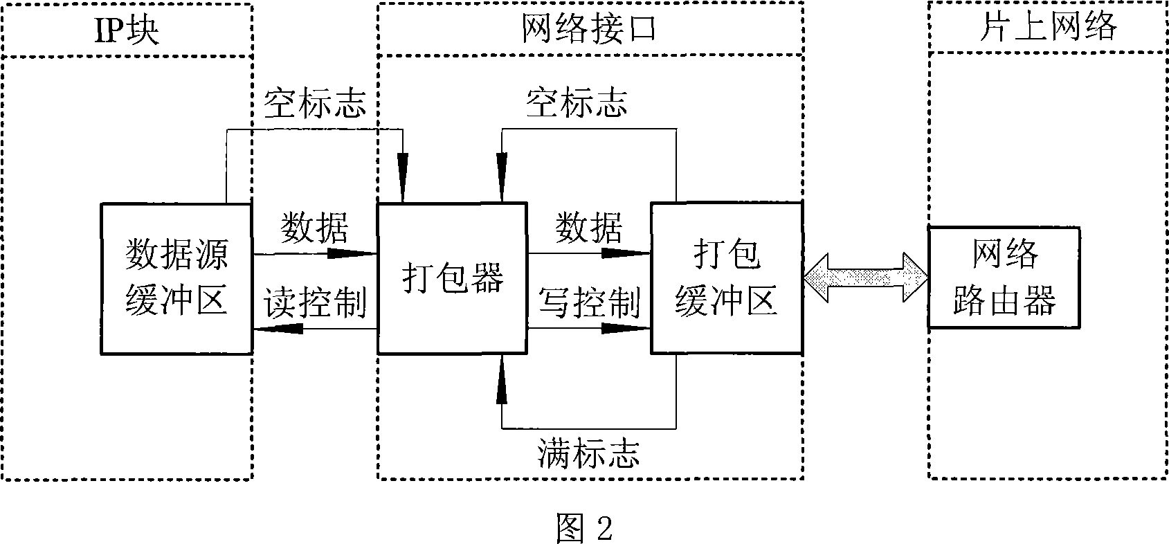
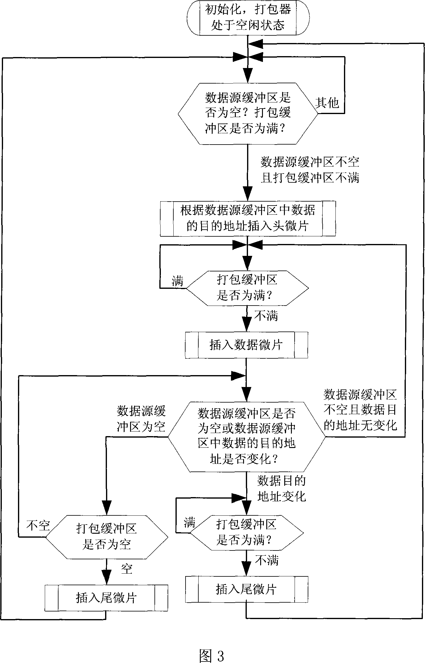
[0025] Embodiment: Figure 3 is a flow chart of the packaging process of the packager. After the packer is initialized, the packer is idle. In the idle state, in each clock cycle, the packer detects the empty flag signal of the data source buffer and the full flag signal of the packed buffer. If the data source buffer is not empty and the packed buffer is not full, the packer buffers according to the data source The destination address of the data in the area is inserted into the head microchip, and the body microchip containing the data is inserted in the next clock cycle when the packing buffer is not full, and the packer enters a busy state. In the busy state, if the data source buffer is not empty, the packing buffer is not full, and the destination address of the data in the data source buffer remains unchanged, the packer will continue to insert volume flakes; if the destination address of the data source data changes, then When the packaging buffer is not full, insert t...


PUM


Abstract

The method feature the following: setting up a data source buffer area at IP block; setting up a packager and a packaging buffer area at the network interface; after system initiation, the packager is at a idle state; when the data source buffer area is not empty and the packaging buffer area is not full, the packager inserts header and tailor and body micro plate, and enters into the busy state; if the data source buffer area is not empty and the packaging buffer area is not full, and the destination address of the data is not changed, the packager inserts the body micro plate; if the destination address in the data buffer source area is changed or the data source buffered area and the packaging buffer area both are empty, the packager inserts the body micro plate and enters into idle state.

Description

technical field [0001] The invention belongs to the field of on-chip interconnection network design. Background technique [0002] Integrated circuits have been advancing in accordance with Moore's Law. The number of TP (Intellectual Property) blocks integrated in a single chip is increasing. The traditional bus-based on-chip interconnection structure has already performed better in terms of bandwidth, power consumption, reliability, and scalability. Increasingly, on-chip communication has replaced computation as the bottleneck in IC design. Network-on-Chip (NoC), as a key technology in the field of integrated circuit design, is used to solve the problem of on-chip interconnection caused by the increase in chip size. [0003] Packet switching is widely used in the design of network-on-chip because of its advantages such as high link utilization. Wormhole routing is also unanimously recommended by network-on-chip researchers because of its advantages in area and delay. In ...

Claims


Application Information

Patent Timeline
Patent Type & Authority Applications(China)
IPC IPC(8): H04L12/56H04L29/02H04L12/861
Inventor 林世俊曾烈光金德鹏苏厉
Owner TSINGHUA UNIV
Why Eureka
Try Eureka