A making method for nano coulomb structure

A nanoscale, tunnel junction technology, applied in the field of preparation of nanoscale Coulomb island structure, can solve the problems of poor reliability, high preparation cost, complicated preparation process, etc., and achieve the effect of increasing the working temperature, reducing the preparation cost and improving the preparation efficiency

Inactive Publication Date: 2007-12-12
INST OF MICROELECTRONICS CHINESE ACAD OF SCI
View PDF5 Cites 8 Cited by
  • Summary
  • Abstract
  • Description
  • Claims
  • Application Information

AI Technical Summary

Problems solved by technology

[0008] 1. The preparation process is complex;
[0009] 2. High preparation cost;
[0010] 3. The preparation efficiency is low and cannot be mass-produced;
[0011] 4. The randomness of preparing the Coulomb island structure is large and the reliability is poor;
[0012] 5. The feasibility of preparing the Coulomb island structure is poor

Method used


Image

  • A making method for nano coulomb structure
  • A making method for nano coulomb structure
  • A making method for nano coulomb structure

Examples


Embodiment 1

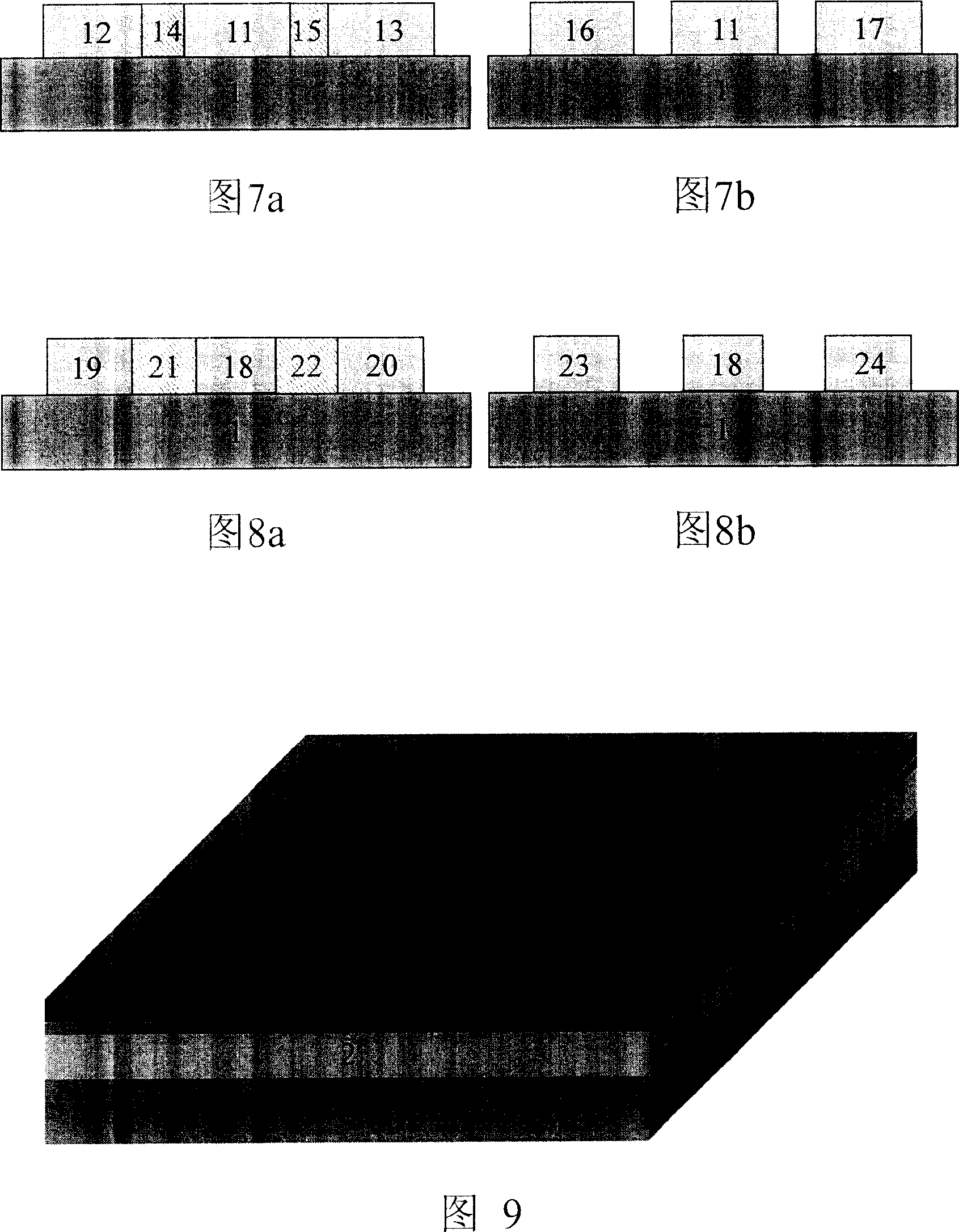
[0092] This embodiment uses heavily doped SOI substrate, SAL601 chemically amplified negative electron resist, and ICP etching method, and further illustrates the detailed process and steps of the present invention in conjunction with the accompanying drawings.

[0093] As shown in FIG. 9, FIG. 9 is a schematic diagram of coating an electronic resist SAL601 on an SOI substrate. Coat SAL601 on a heavily doped n-type, (111) crystalline SOI substrate (consisting of three layers of silicon substrate 1, 160nm thick buried oxide layer 2 and 80nm thick top layer silicon 3 from bottom to top) Negative chemically amplified electronic resist 4 was applied at a rotation speed of 3000 rpm, and pre-baked at 120° C. for 3 minutes using a hot plate.

[0094] As shown in FIG. 10 , FIG. 10 is a schematic diagram of forming a Coulomb island structure in electronic resist SAL601. Electron beam direct writing exposure, post-baking, and development are used to form Coulomb island structure patter...

Embodiment 2

[0098] In this embodiment, a heavily doped SOI substrate, ZEP520 positive electron resist, and ICP etching are used. In this embodiment, except for some conditions of EBL, other conditions are the same as those in Embodiment 1. The pre-baking conditions are baking at 160°C for 35 minutes in an oven; the exposure dose is 130 to 160μC / cm 2 ; no post-baking required; developed with amyl acetate for 4 minutes at room temperature and fixed with 4-methylpentanone 2 (MIBK) for 30 seconds at room temperature.

[0099] Fig. 13 is an actual SEM photo of the core part of the Coulomb island structure after ICP etching in the second embodiment of the present invention. The gray background in the figure is the buried oxide layer 2 of the SOI substrate; the white part corresponds to the top silicon layer 3 of the SOI substrate, and the middle point is the unoxidized Coulomb island 13, and the slightly larger figures on the left and right sides are the source 11 and drain 12, the part where...


PUM

PropertyMeasurementUnit
diameteraaaaaaaaaa
diameteraaaaaaaaaa

Abstract

The invention discloses a preparing method of nanometer-class coulomb island structure, it includes: A. smearing electron slushing compound on conducting layer of underlay; B. baking the electron slushing compound; C. electron beam exposing the electron slushing compound; D. imaging the electron slushing compound exposed; E. fixing the electron slushing compound imaged; F. process of glue-eliminating and high temperature oxidation is proceeded to coulomb island structure obtained to obtain nanometer-class coulomb island structure whose size is more smaller. With the invention, preparing craftwork is simplified, cost is decreased, efficiency is increased, and reliability of coulomb island structure is increased. The preparing method provided in the invention possesses advantages that it is compatible with traditional CMOS, fits for the extending and application.

Description

technical field [0001] The invention relates to the technical field of nano-electronic devices and nano-processing, in particular to a method for preparing a nano-scale Coulomb island structure for making single-electron devices. Background technique [0002] Integrated circuits with complementary metal oxide semiconductor (CMOS) devices as the mainstream technology have been following Moore's law and developed rapidly. In 2004, integrated circuits entered the 90nm technology node. As the feature size enters the nanoscale, the traditional CMOS technology is facing more and more serious challenges. Therefore, nanoelectronic devices based on new principles have become a research hotspot. [0003] Single-electronic devices have the advantages of small size, fast speed, low power consumption, and large-scale integration, and have very broad application prospects, such as making single-electronic memory, single-electronic logic circuits, current standards, ultra-sensitive electro...

Claims


Application Information

Patent Timeline
Patent Type & Authority Applications(China)
IPC IPC(8): H01L21/335G03F7/00
Inventor 龙世兵陈杰智李志刚刘明陈宝钦
Owner INST OF MICROELECTRONICS CHINESE ACAD OF SCI
Why Eureka
Try Eureka