Film transistor with copper wire structure and its manufacturing method

A technology of thin film transistors and manufacturing methods, applied in the direction of transistors, semiconductor/solid-state device manufacturing, semiconductor devices, etc., can solve problems such as difficult etching results, poor adhesion of insulating substrates, component failures, etc., to simplify the patterning process and reduce resistance value effect

Inactive Publication Date: 2007-12-19
台湾薄膜电晶体液晶显示器产业协会 +7
View PDF0 Cites 16 Cited by
  • Summary
  • Abstract
  • Description
  • Claims
  • Application Information

AI Technical Summary

Problems solved by technology

However, the adhesion of copper to the insulating substrate is poor, and Cu ions are easy to diffuse to the active layer, resulting in component failure. In order to increase the adhesion between Cu and the underlying layer and inhibit the diffusion of copper ions, metals such as Mo, Ti, and Ta are often used to form cladding layers. However, in the etching process, two metal layers need to be etched separately. If you want to use a single etching solution to etch the multi-layer metal, it is difficult to achieve ideal etching results due to the different types of metals.
[0003] In addition, if only copper alloy is used as the metal gate, although the copper alloy has been proven to inhibit the diffusion of copper ions and has a good adhesion effect with the substrate, but the copper alloy has a high resistance value and high manufacturing cost of the target. still have doubts about the application

Method used


Image

  • Film transistor with copper wire structure and its manufacturing method
  • Film transistor with copper wire structure and its manufacturing method
  • Film transistor with copper wire structure and its manufacturing method

Examples


Embodiment Construction

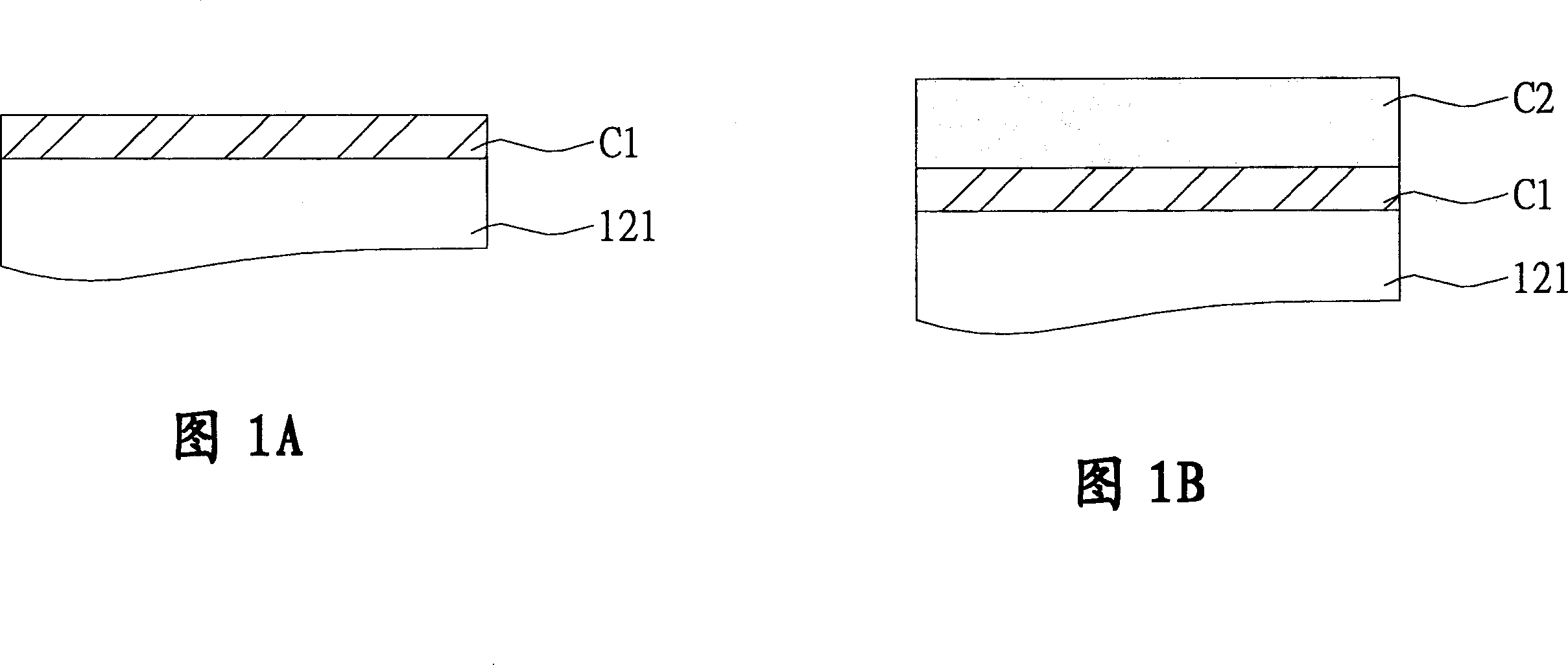
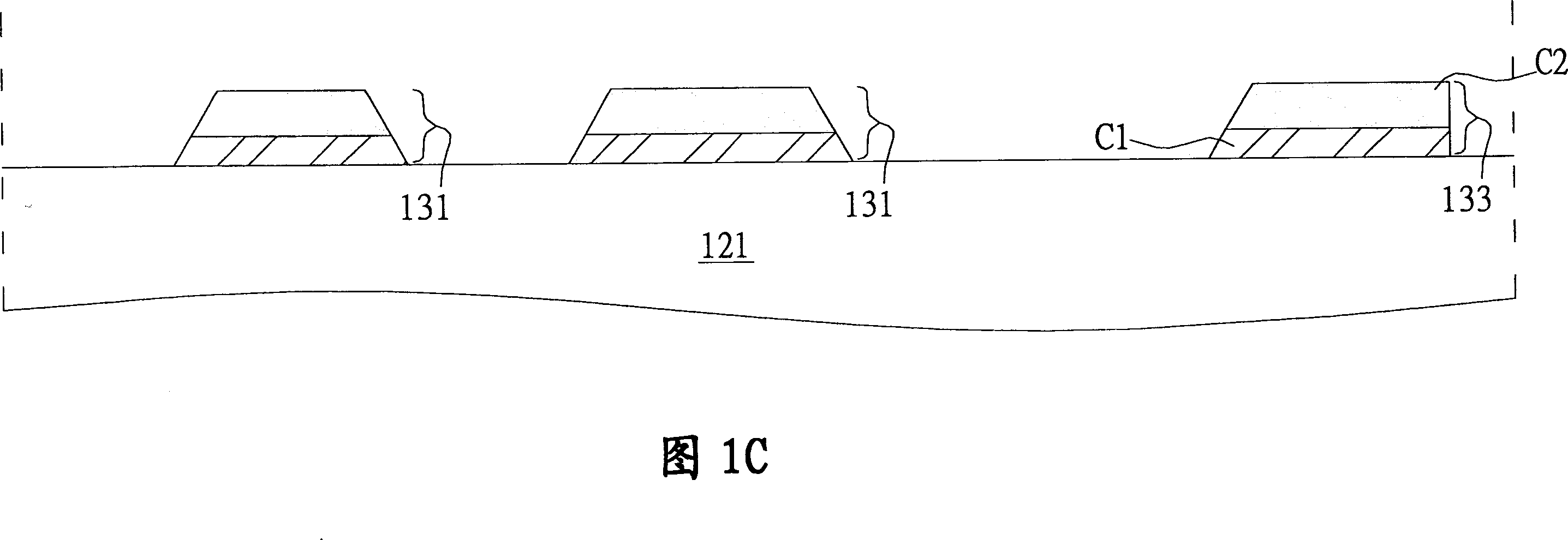
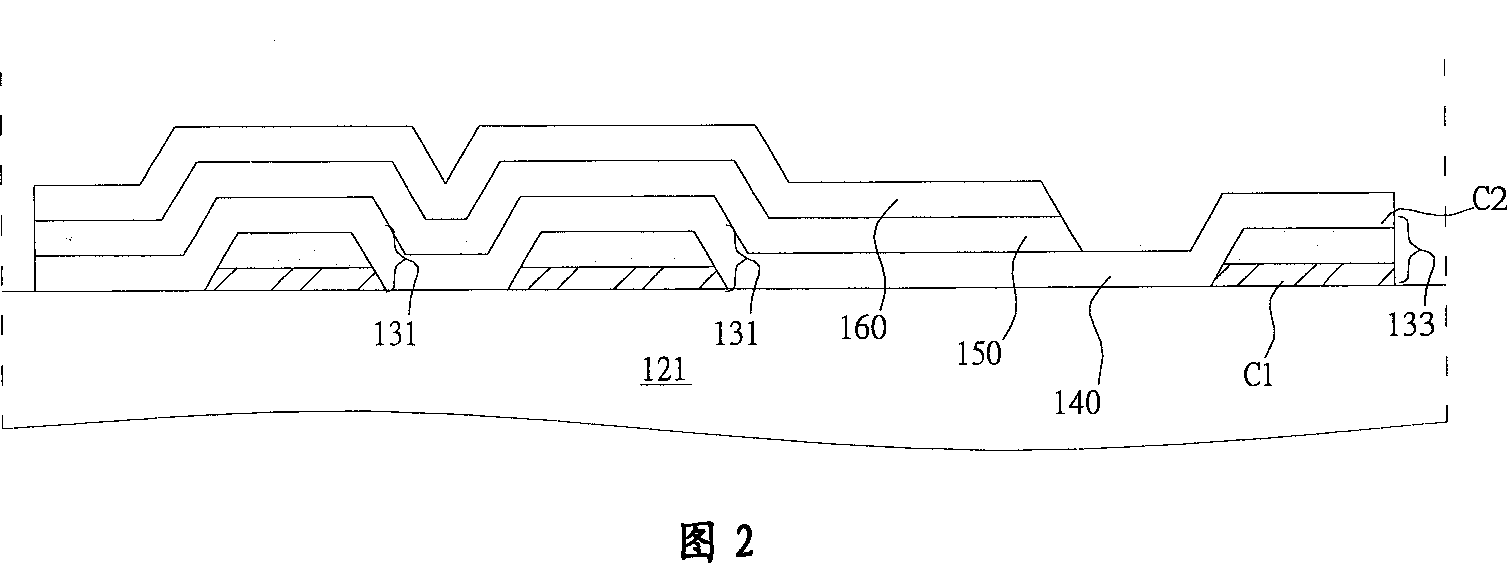
[0025] Please refer to FIG. 1A to FIG. 1C , which are process cross-sectional views of the gate of the double-layer metal structure of the present invention.

[0026] First, in an embodiment of the present invention where the gate 131 and the gate line 133 are generated, as shown in FIG. 1A to FIG. 1B , a substrate 121 is sequentially deposited to form a A copper alloy layer (copper alloy layer) C1 with a thickness of about 10 to 2000 angstrom and a copper layer (copper layer) C2 with a thickness of about 1000 to 4000 angstrom. Then, as shown in FIG. 1C, define the pattern of the double-layer metal structure such as the formed copper alloy layer C1 and copper metal layer C2, so as to produce a copper wire of the double-layer metal structure, and then perform heat treatment at a temperature of about 100 to 500° C. (heat treatment).

[0027] In another embodiment of the present invention for generating the gate 131 and the gate line 133, as shown in FIG. 1A to FIG. 1B, a layer ...


PUM

PropertyMeasurementUnit
thicknessaaaaaaaaaa
thicknessaaaaaaaaaa

Abstract

This invention relates to a film transistor with a copper lead structure and its manufacturing mehod, which utilizes at least one copper alloy layer and a copper layer to form a grid with multiple metal structures to improve atom arrangement among lattice interfaces and keyed jointing among atoms and reduce resistance values to suppress diffusion of Cu ions after heat process to get better electric conductance of film transistors, besides, when figuring the multiple metal thin layers, it' s only necessary to use single layer of Cu etching liquor to simplify the figuring technology.

Description

technical field [0001] The invention relates to a thin film transistor liquid crystal screen, in particular to a thin film transistor with a copper wire structure and a manufacturing method thereof. Background technique [0002] As liquid crystal displays are widely used, the size of the displays is gradually increasing. However, as the size of the display increases, the delay problem of the RC circuit becomes more and more serious, so copper metal with low resistance value is developed as the wire. However, the adhesion of copper to the insulating substrate is poor, and Cu ions are easy to diffuse to the active layer, resulting in component failure. In order to increase the adhesion between Cu and the underlying layer and inhibit the diffusion of copper ions, metals such as Mo, Ti, and Ta are often used to form cladding layers. However, in the etching process, two metal layers need to be etched separately. If a single etching solution is used to etch the multi-layer metal,...

Claims


Application Information

Patent Timeline
Patent Type & Authority Applications(China)
IPC IPC(8): H01L27/12H01L23/522H01L29/786H01L29/49H01L21/84H01L21/768H01L21/336H01L21/28
Inventor 吴健为梁硕玮陈琬琪杨承慈刘思呈王敏全官永佳
Owner 台湾薄膜电晶体液晶显示器产业协会
Why Eureka
Try Eureka