Aluminium and lead laminar composite material
A composite material and lead layer technology, applied in the direction of metal layered products, layered products, electrodes, etc., can solve the unfavorable comprehensive performance of lead electrode materials composed of lead alloys, can not solve the problem of titanium-lead interface bonding, lead electrochemical performance Advantage weakening and other problems, to achieve the effect of reducing electrode internal resistance, weight reduction, and performance index improvement
- Summary
- Abstract
- Description
- Claims
- Application Information
AI Technical Summary
Problems solved by technology
Method used
Image
Examples
Embodiment 1
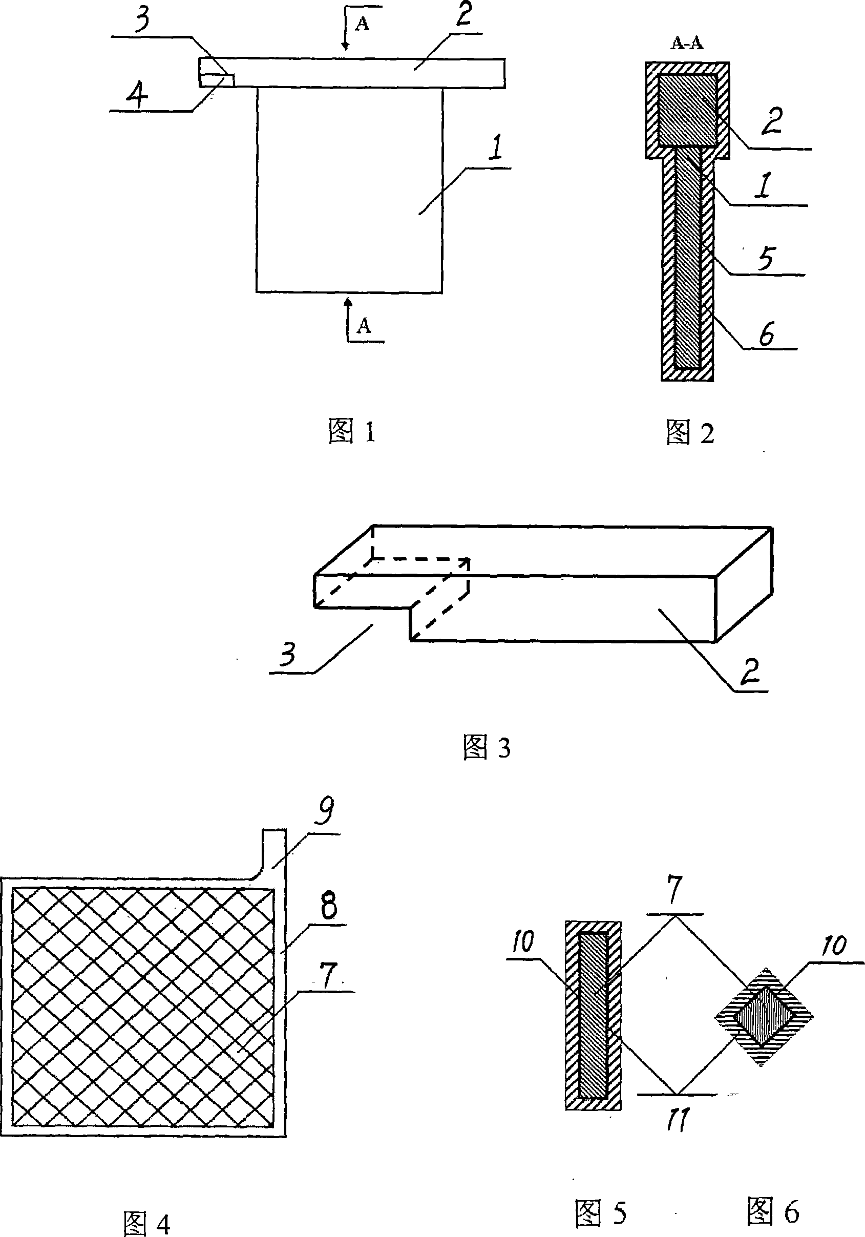
[0021] Use industrial aluminum plate with a thickness of 1mm to make an anode plate core 1 with an overall dimension (length×width) of 1025mm×630mm, which is slightly smaller than the traditional standard anode plate, and then use a 10mm thick industrial aluminum row to make an anode plate core 1 with a length×width of 1054mm×50mm Conductive beam 2, at one end of the conductive beam 2, cut off a copper lug interface end 3 with a length × width × thickness of 120 mm × 8 ~ 10 mm × 25 mm, and use the current aluminum-copper composite method on the cut aluminum conductive beam interface A piece of conductive copper tab 4 with a length×width×thickness of 120mm×12-16mm×28mm is prepared from the terminal 3 . The aluminum core board 1 is welded at the center position of the length direction of the conductive beam 2 to form a whole. After the welded core board 1 and the conductive beam 2 are subjected to surface removal treatment in the prior art, a layer with a thickness of A tin tran...
Embodiment 2
[0023] After the industrial aluminum plate with a thickness of 0.4 mm is used to draw mesh 7, it is cut according to the required capacity lead storage battery grid dimensions (length × width) and prepared into a complete grid shape with frame 8 and tabs 9, As the aluminum core, after the surface of the aluminum core grid is pretreated, a layer of 40 μm antimony transition alloy layer 10 is formed on it, and then the outer surface of the antimony transition alloy layer 10 is coated with a layer of Pb- Sb-As-Se lead alloy layer 11, and the grid meshes are not filled with lead alloy, as shown in Fig. 4, Fig. 5 and Fig. 6.
PUM
| Property | Measurement | Unit |
|---|---|---|
| thickness | aaaaa | aaaaa |
| diameter | aaaaa | aaaaa |
| thickness | aaaaa | aaaaa |
Abstract
Description
Claims
Application Information
