Method for restraining edge breakdown of avalanche photodiode

An avalanche photoelectric and diode technology, which is applied in the manufacture of circuits, electrical components, semiconductors/solid-state devices, etc., can solve problems such as difficulty, limit chip size, and complex implementation, and achieve the goal of suppressing and preventing edge breakdown Effect

Inactive Publication Date: 2007-12-26
GUANGZHOU LEDY LIGHT
View PDF0 Cites 8 Cited by
  • Summary
  • Abstract
  • Description
  • Claims
  • Application Information

AI Technical Summary

Problems solved by technology

This technology involves a variety of processes, including secondary growth, reactive ion etching, etc., and the implementation is relatively complicated.
[0006] Traditional techniques for suppressing edge breakdown of APD devices require complex processes such as secondary diffusion, ion implantation, or secondary growth. These processes are relatively difficult for small-sized chips, especially Guard ring technology largely limits the size of the chip

Method used


Image

  • Method for restraining edge breakdown of avalanche photodiode
  • Method for restraining edge breakdown of avalanche photodiode
  • Method for restraining edge breakdown of avalanche photodiode

Examples


Embodiment 1

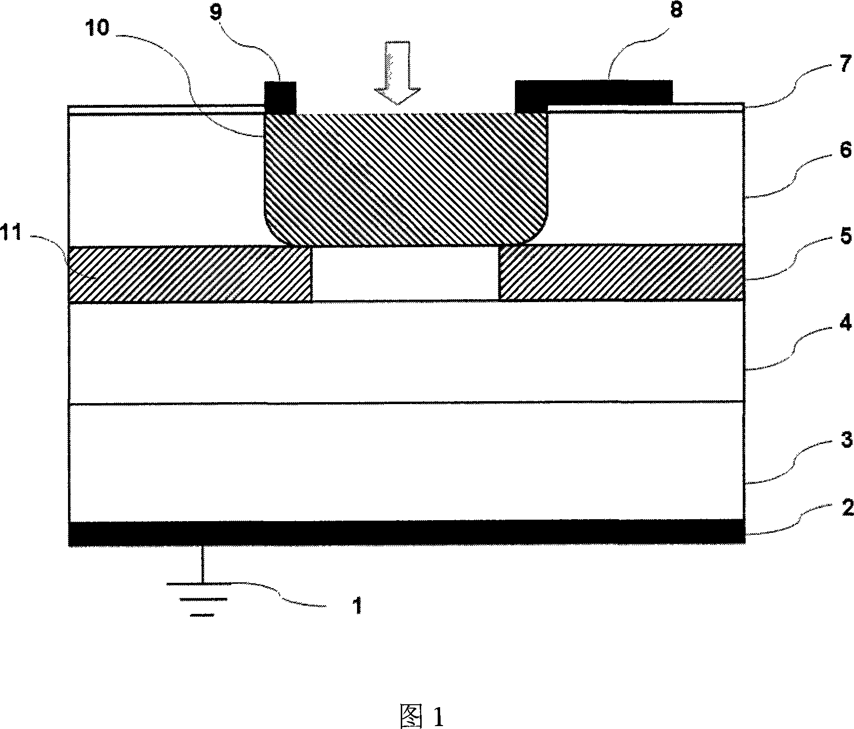
[0029] As shown in Figure 2, the APD structure with front light incident, the substrate 3 is GaAs material (gallium arsenide), the absorption layer 4 is GaInNAs material (gallium indium nitrogen arsenide), and the multiplication layer 5 is AlGaAs material (aluminum gallium arsenide) , The intrinsic substrate layer 6 is GaAs material. Choosing GaInAs material for the absorption layer 4 can control the width of the bandgap by adjusting the composition of In and N so that the wavelength of the absorbed light falls in the optical communication band; choosing AlGaAs material for the multiplication layer 5 can effectively control the multiplication noise. In the process of process realization, firstly, the GaInNAs absorption layer 4, the AlGaAs (x>0.8) multiplication layer 5 with high aluminum composition and the intrinsic substrate layer 6 can be grown sequentially on the N-type GaAs substrate 3 by MOCVD, and then by diffusion A P-type heavily doped region 10 is formed on the intri...

Embodiment 2

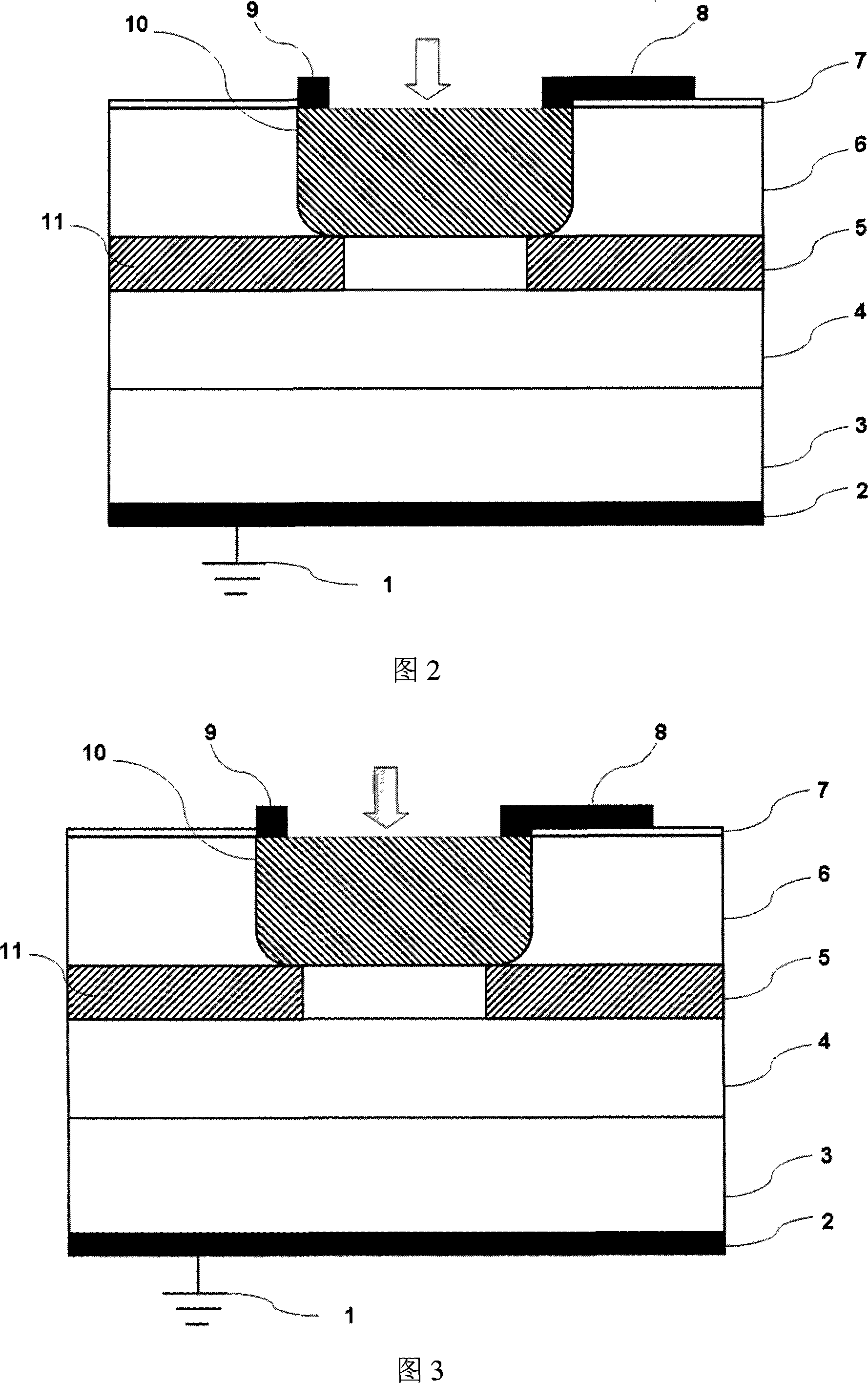
[0031] Figure 3 shows the APD structure with front light incident, the substrate 3 is made of InP material (indium phosphide), the absorption layer 4 is made of GaInAs material, the multiplication layer 5 is made of GaAlInAs material, and the intrinsic substrate layer 6 is made of InP material. Since the InGaAs material matched with InP absorbs in the optical communication band, and its SCAM structure has good bandwidth characteristics, it is widely used in optical communication systems. The process of technological realization is identical with embodiment 1.

Embodiment 3

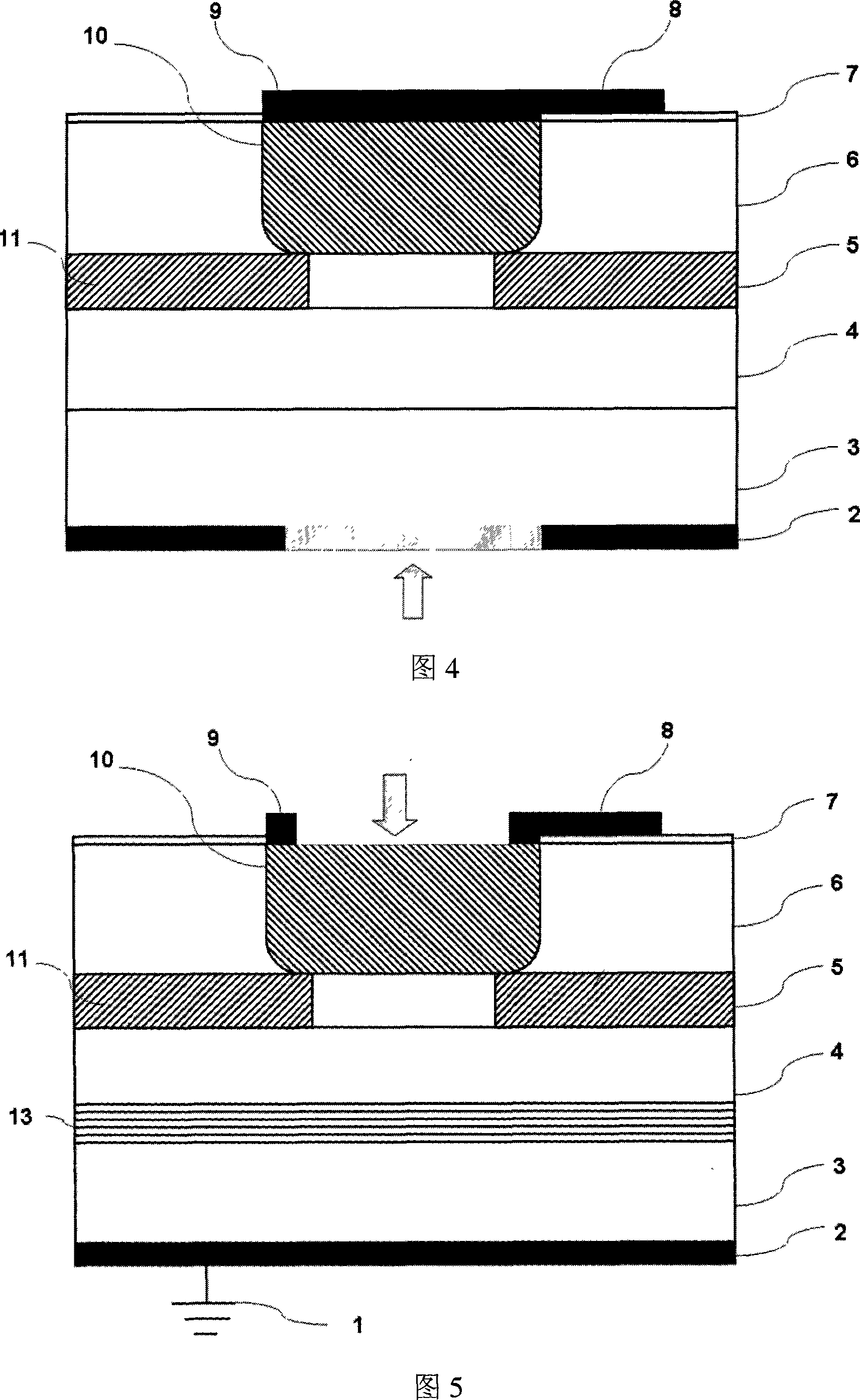
[0033] Figure 4 shows the APD structure with back light incident, the substrate 3 is made of GaAs material, the absorption layer 4 is made of GaInNAs material, the multiplication layer 5 is made of AlGaAs material, and the intrinsic substrate layer 6 is made of GaAs material. The manufacture of the main structure in terms of technology is the same as that of Embodiment 1, the difference lies in the manufacture of electrodes. In this embodiment, the P-type electrode 8 and the P-type electrode 9 are directly fabricated on the P-type heavily doped region 10. When fabricating the N-type electrode 2, a substrate 3 is etched on the substrate 3 by semiconductor photolithography to receive incident light. window, and evaporate an anti-reflection metal film, and finally make an N-type electrode 2.


PUM


Abstract

The method includes steps: (1) material of containing high aluminum component (AC) is selected for multiplier layer in structure of avalanche photodiode, material of containing no or low AC is selected for absorbing layer; (2) first, oxidizing material of containing high AC at lateral edge in the multiplier layer, and then making insulating layer of alumina expand to P type heavily doped area from lateral direction. The invention restrains edge breakdown by using insulating layer formed from selective oxidation reaction between water vapor etc of oxygen-containing material and multiplier layer material with high AC. Compared with traditional second diffusion, second growth, the disclosed technique is simpler. Accurate controlled length of oxidation, and formed insulating layer material prevent edge breakdown caused by effect of curvature in P diffusion area. The invention does not need to make specific structure (such as guard ring) so as to not limit size of chip.

Description

technical field [0001] The invention relates to an avalanche photodiode, in particular to a method for suppressing edge breakdown of an avalanche photodiode. Background technique [0002] In the past five centuries, avalanche photodiodes (APDs) have been widely used in commercial, military and scientific research. In recent years, with the rapid development of the optical communication industry, photodetectors, which play an important role in receivers in optical communication systems, have also developed rapidly. Sensitivity in the receiver is one of the important indicators in the optical communication system. Impact ionization will occur inside the APD to form an internal gain, which is 5-10dBm better than the sensitivity of the traditional photodiode (PIN), making the APD the first choice for the receiver in the optical communication system. . [0003] From the 2.5Gbit / s transmission rate of traditional optical communication to the current 40Gbit / s transmission rate, t...

Claims


Application Information

Patent Timeline
Patent Type & Authority Applications(China)
IPC IPC(8): H01L21/329
Inventor 王钢陈诗育
Owner GUANGZHOU LEDY LIGHT
Why Eureka
Try Eureka